
Conducted Emission Test Background
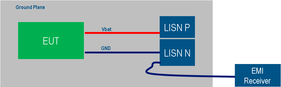
The conducted emission (CE) test consists of a measurement of current on wires or a voltage across the Line Impedance Stabilization Network (LISN) measurement port. In the automotive field, the test setup is composed of the Equipment Under Test (EUT), wires, LISN, EMI (Electromagnetic interference) receiver, a communication device such as CAN, a load (if necessary) and the ground plane, which represents the chassis of the car and represents a voltage reference.
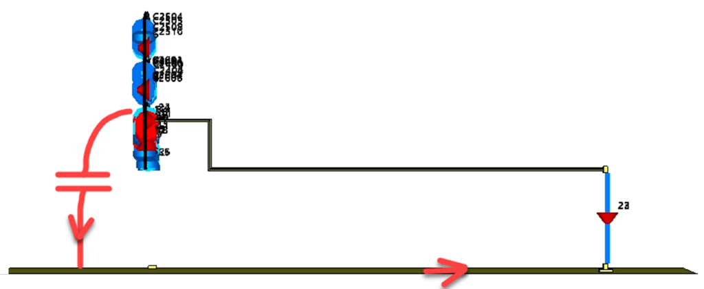
Figure 1 describes a simple test setup: Vbat and GND represent wires for positive and negative polarities of the power supply, respectively. The EUT in our case is a simple “Printed Circuit Board” (PCB) but it could represent any other electrical or electronic system. The EMC performance during CE testing consists of a comparison of the measured voltages/currents to the limits defined by a standard such as CISPR 25, which is the most applied standard in the automotive field. In our case, we focus on the voltage method. The choice of measurement is not a limitation, since testing by voltage method and by the current method are equivalent.
EUT Description
In this study, the EUT is a simple PCB composed of multiple ground layers and with one trace excited by a signal. We use it to illustrate the coupling between the trace and the ground plane and how the layout impacts this coupling. We study three cases:
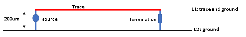
- Case 1 consists of a 2-layer PCB. The excited trace is on the bottom layer. The top layer is the PCB ground reference (see Figure 2).
- Case 2 consists of a 4-layer PCB with the excited trace between two solid PCB reference layers for the propagating signal (see Figure 3).
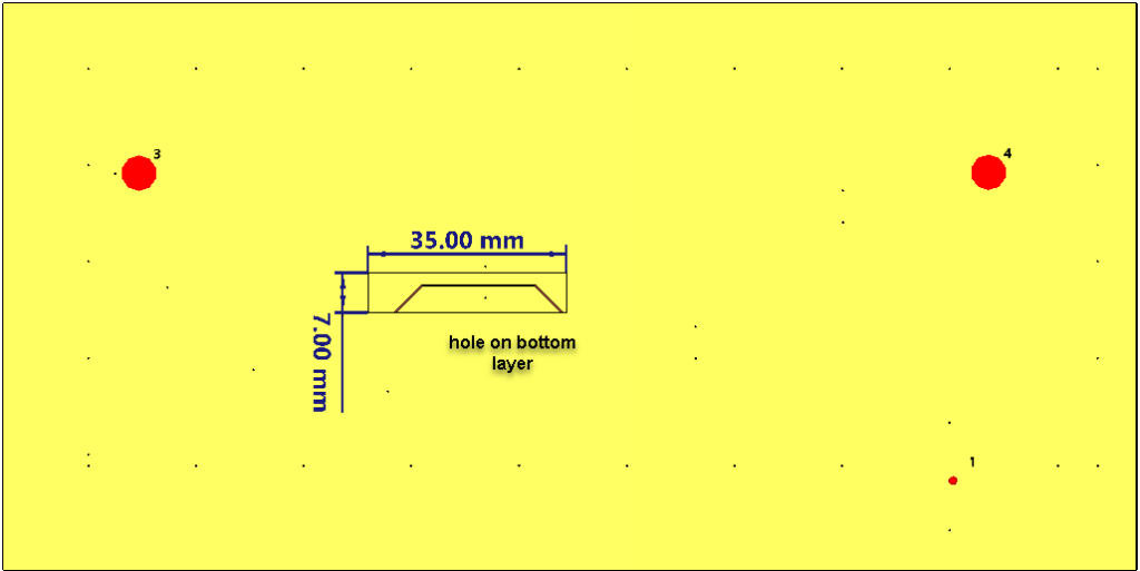
- Case 3 is the same as case 2, with a hole on the bottom layer just underneath the trace (see Figure 4).
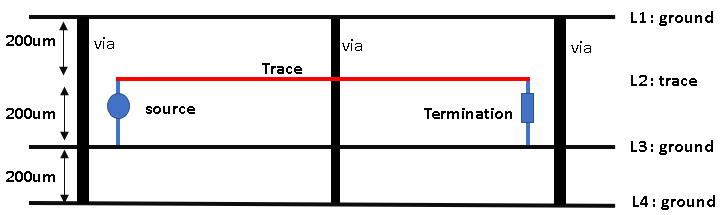
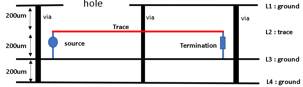
Case 2 and case 3 are simplified to three layers instead of four. Indeed, L4 is suppressed to simplify the model and make the interpretation of the result easier. This simplification doesn’t impact the final result as there is no noise source between L3 and L4 and the voltage that could exist between them is neglectable. The ground layer could also be a power layer connected through decoupling capacitors. In our case, the capacitors are considered as perfect and layers are connected to each other using multiple vias to have a minimum impedance between them. The PCB model with three layers is therefore representative of the full 4-layer system.
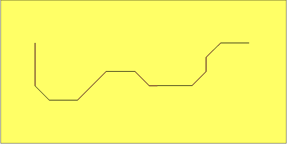
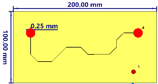
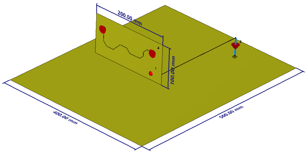
The PCB has a rectangular form and dimensions of 21 cm by 10 cm, the trace length is equal to 21 cm and its width is equal to 0.25 mm as seen in Figure 5.
Conducted Emission Test Setup
The setup is composed of the PCB and a connection of the PCB reference to the LISN impedance through a 20-cm long wire. Usually, the power supply is connected to PCB using two wires: one for negative polarity and another one for positive polarity. In our study, we replace these power supply wires by only one, the ground wire.
Only the common mode is considered in this study, which is the most dominant mode for the coupling. In fact, the input impedance between negative and positive wires is negligible. They are usually connected by a capacitor, which is assumed to be ideal in this study.
The 3D model of test setup is depicted in Figure 6. The board is oriented vertically, the trace is on the bottom layer and the ground wire is connected to the top layer. There is no local ground connection between the PCB and the ground plane.
Noise Source and Termination
The trace is excited by a signal coming from a buffer or micro-controller and terminated by a fixed impedance. It models a clock or a communication signal with some high frequency component. In the simulation, the excitation is a wideband voltage source in the frequency range from 100 kHz to 300 MHz. The termination is a 50-kΩ resistor. Regarding the studied frequency range, the exact value of termination impedance is not important but it is high enough to make the capacitive coupling more dominant.
Simulation Method
For the 3D simulation, the full-wave frequency domain (FD) solver is used. It is the best choice for analyzing PCBs in the frequency range from 100 kHz to 200 MHz. At first, the 3D model is built, meshed and solved using the FD solver. Then, we use a co-simulation with the schematic of the CST Studio Suite to perform a circuit simulation based on the results of the 3D simulation.
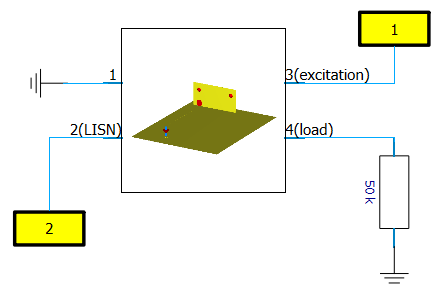
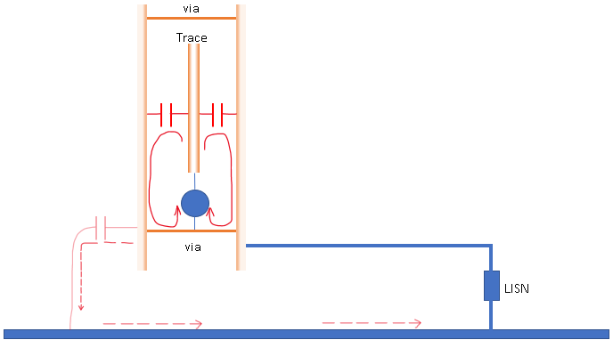
The configuration is separately defined in terms of impedance and components connected to each port that we want to analyze. This means that we can change the termination and driving values and obtain the LISN voltage without solving the 3D model every time again. This reduces the simulation time significantly. Also, in the co-simulation design flow, we can use the “combine result” feature to calculate the current and EM field in the 3D model considering all driving and termination circuitry. This visualization is useful for investigation. It allows a deep analysis of the coupling process for every simulated configuration. The studied circuit is simple and described in Figure 7.
We note that in the simulated cases the GND wire is directly connected to the PCB but it can be disconnected or connected through any impedance like a CMC “Common Mode Choke” as it could be the case in many designs.
Simulation Results
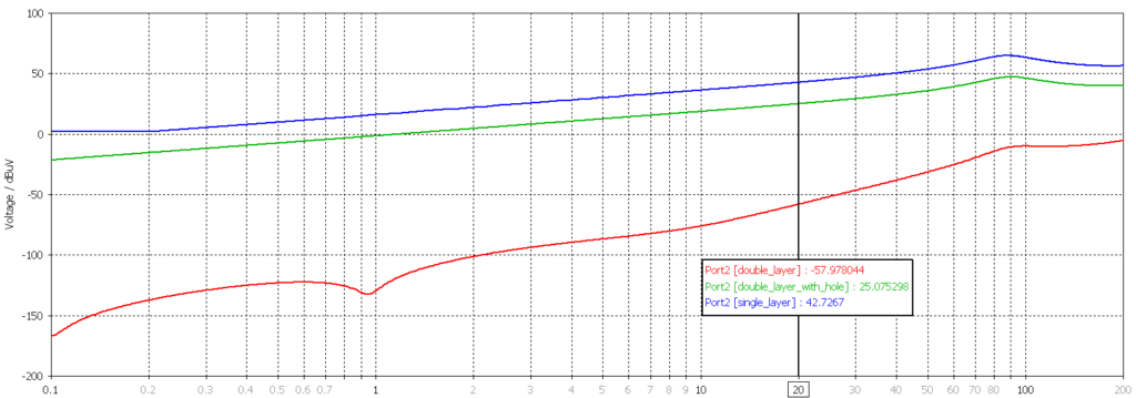
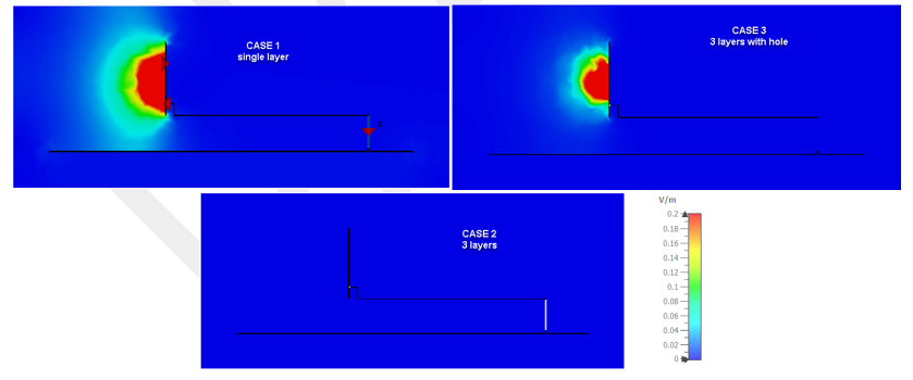
We analyze the voltage across the LISN when the trace was excited by a 1-V broadband noise source using the AC analysis. The results obtained are presented in Figure 8. In case 1 “single layer” the coupling ratio is 78 dB, it means that for 1 V applied to the trace we get 42 dBµV at 20 MHz, which is above the requirement of CISPR 25 conducted emission class 5 “Narrow band noise”. This level is reduced to -58 dBµV in case 2 “double layer”, which is a very low level. In case 3 “trace with hole”, the coupled level is 25 dBµV, it represents an increase of 83 dB compared to case 2. Indeed, case 3 represents a high risk for conducted emission according to CISPR 25 class 5. The whole results show that the hole on a ground layer above or underneath the trace reduces the improvement we have obtained by the use of 3 or 4 layers by 82 dB (from -58 dBµV to 25 dBµV) which would be extremely difficult to deduce without the use of 3D simulation.
Analyzing the Coupling Mechanism
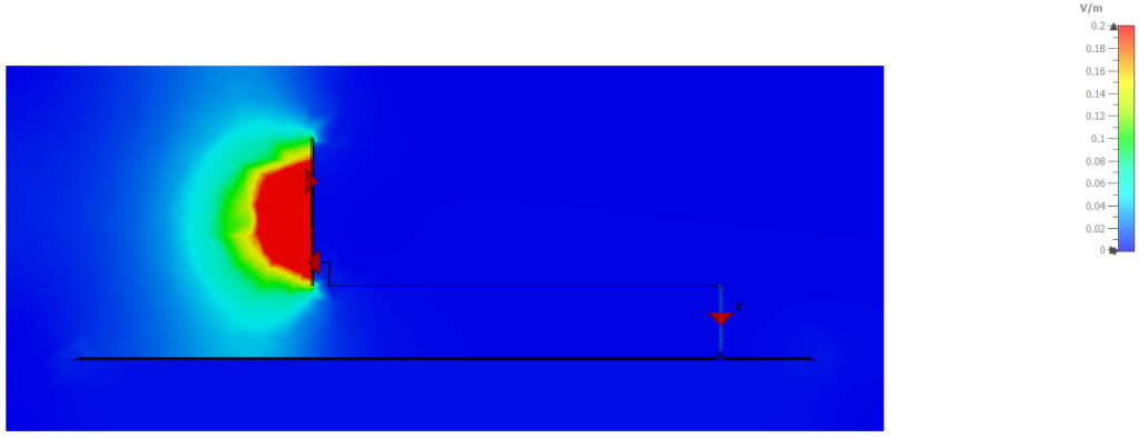
The first question that immediately pops up at this point is: How can there be a current on the LISN knowing even there is only one connection between the PCB and the ground plane? To answer this question, we can use an E field monitor at 20 MHz, see Figure 9. We can notice clearly that there is an electrical field between the PCB and ground plane. The variation of this field induces a displacement current through the stray capacitance between the PCB and ground plane as indicated by Figure 10. This displacement current induces a voltage in LISN impedance.
When the trace is buried between two ground layers as in case 2, the coupling between the trace and ground plane is hugely decreased. In fact, the coupling between the trace and ground layers increases significantly and changes the current distribution to be localized between the inner layers. As the electric field is confined between trace and PCB layers, there is no current at the outer faces of the PCB layers and there is no field between them and the ground plane. This decreases the coupling between the PCB and the ground plane.
When the PCB layers contain a hole above the trace as in “case 3”, the coupling level becomes close to the one of case 1 “single layer” Figure 12. The difference is only 33 dB. Obviously, this value changes as a function of the position and size of the hole.
Conclusion
We have used a 3D simulation to study the coupling between PCB and ground plane in a conducted emission test setup. The results show that the trace terminated by high impedance generates an electric field between it and ground plane, which induces a displacement current and voltage on LISN impedance. This coupling is hugely reduced when the trace is routed between two inner layers. However, the improvement could be significantly compromised by the presence of a hole in one of the ground layers above or underneath the trace. This conclusion is quite surprising: even a small hole above a short section of the PCB can degrade the improvement significantly. With the proposed simulation workflow, it is very straightforward to study alternative configurations by, for example, changing driving and termination impedances or modifying the layout of the PCB.

Interested in the latest in simulation? Looking for advice and best practices? Want to discuss simulation with fellow users and Dassault Systèmes experts? The SIMULIA Community is the place to find the latest resources for SIMULIA software and to collaborate with other users. The key that unlocks the door of innovative thinking and knowledge building, the SIMULIA Community provides you with the tools you need to expand your knowledge, whenever and wherever.

Djamel Guezgouz joined Dassault Systeme France since June 2023. His current position is SIMULIA Industry Process Senior Consultant with the main focus of EMC simulation. From October 2021 to May 2023, he was an EMC Expert at Great Wall Group, China, where he was responsible on EMC HW design, integration and simulation development of inverter for EV and PHEV cars, as well as EMC test and measurement. He worked 2 years as EMC expert in military field at Arquus SAS France. Before that, he was working 5 years as EMC engineer and 3 years as junior expert at Renault Group France. He was responsible on EMC development of high voltage devices of EV cars, he gave an EMC training and participated to the establish and write of Renault and Nissan EMC standard for high voltage components. He is graduated with PhD degree in electronics from University of Tours in 2010.