
Thermal simulation can reveal the temperature distribution on a PCB before manufacturing a physical prototype. This document will demonstrate a fast, efficient workflow for PCB thermal simulation in CST Studio Suite using IR-Drop analysis and show the advantages of this approach. The simulation results will also be verified against measurements.
This analysis considers a PCB without any enclosure. In order to keep the model preparation stage as simple as possible, all necessary data needed to engage a thermal simulation is obtained from an IR-Drop analysis (e.g. heat sources, thermal losses of a PCB, geometry of the PCB components).
Thermal simulation is run with the CST Studio Suite conjugate heat transfer solver (CHT) as it is the best suited for the job. With this approach a user saves a lot of time during model setup, because the workflow does not require a user to manually search and define equivalent thermal models (e.g. 2-resistor) for each and every single one of the components soldered on the PCB. Moreover, CHT analysis removes the need for the user to set thermal surfaces in the model. Where necessary, AC losses can also be added to the simulation through 3D co-simulation.
Simulation setup and IR-Drop
As shown in Fig.1, the simulation process is relatively simple. Firstly, a user collects all necessary data (e.g. E-, M-CAD models, PCB layout with its stack-up and schematics, PCB component shapes, and so on). Nowadays, almost all of that information is already stored inside files generated by well-known EDA tools.
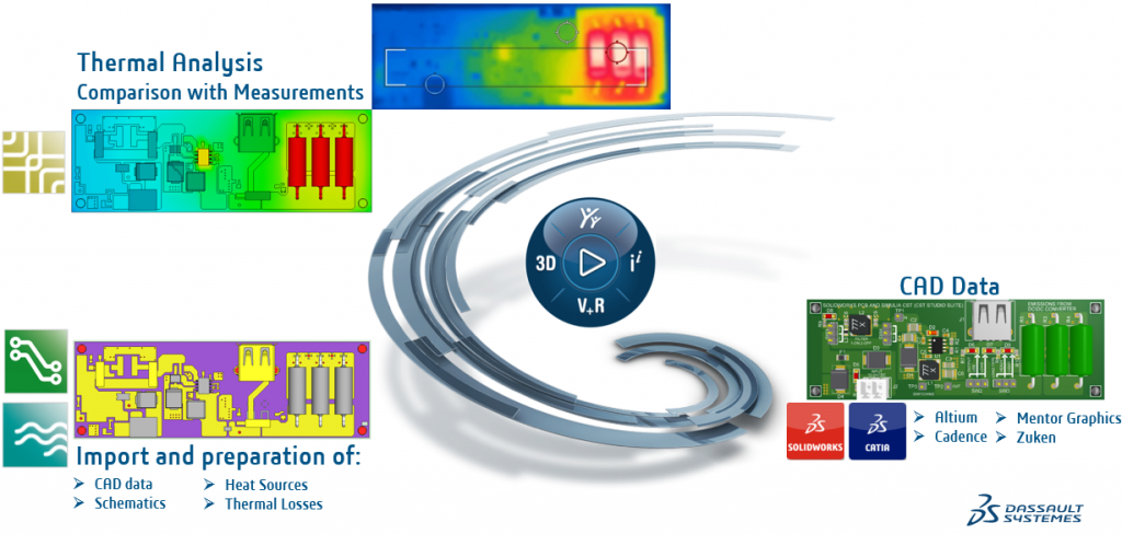
Secondly, a user imports an EDA layout into CST Studio Suite, validates its integrity, and based on its schematics sets up and runs an IR-Drop analysis.
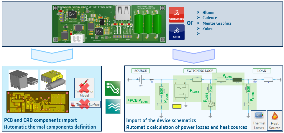
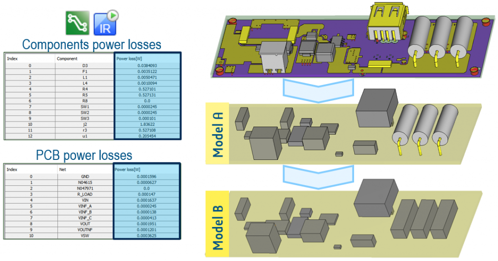
The IR-Drop analysis provides a lot of information for the user to decide the complexity level of the thermal model. For example, it can be seen that calculated power losses within PCB layers are relatively low in comparison to components losses (depicted on Fig.3). Hence the CST Studio Suite stack-up simplification mechanism can be activated in order to create and use a model with equivalent thermal properties but with much less complexity and therefore shorter simulation times.
Thermal Simulation
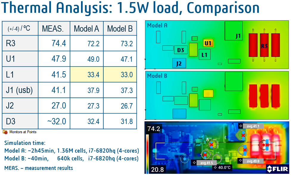
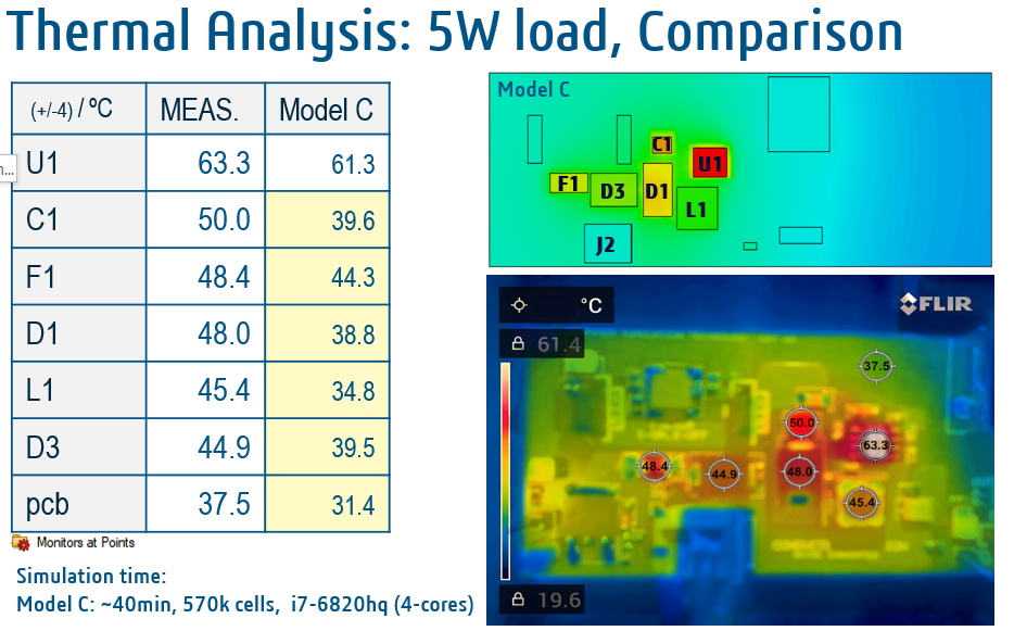
The thermal simulations are performed for two different electrical loading conditions: 1.5 and 5 watts (W).
The models specified for a load 1.5W are shown on Fig. 3 and for 5W on Fig.4.
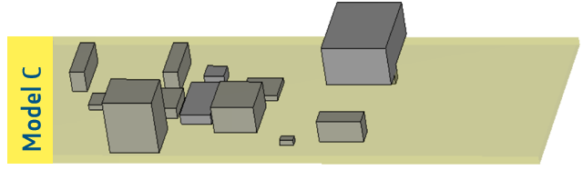
Based on input CAD data, the user can set up and analyze several cases with different complexity of the PCB components (as shown in Fig.3).
For this comparison, the shapes of components are auto-generated by CST Studio Suite to create a simplified version for models A, B and C with one exception in model A, where power resistors are directly imported from CAD database.
Components are characterized by a default material, automatically assigned by the workflow, with a thermal conductivity (TC) of 5W/K/m. An exception is made for the power resistors and connectors (J1,, J2). TC for these components is chosen experimentally based on publicly available information.
The core of a power resistor is generally constructed either from a fiber glass or ceramic material, which leads to a TC in the range of < 0.5 – 3 > W/K/m. The resistor leads are defined as copper with a TC of 401W/K/m.
Connector J2 is made out of a dielectric material with a TC of 1.5W/K/m.
The simulation model of a USB connector (J1) is simplified. Its shell is modelled as aluminum with a TC of 237W/K/m and its “insides” are estimated as a material with a TC of 1.5W/K/m.
None of the PCB components contain a thermal pad, therefore all of them are assigned with a contact property towards the PCB stack-up. The experimentally measured thickness of the air gap varies in the range of < 50 – 200 > μm.
50μm is used in the simulation.
Remark 1: Three power resistors (through-hole type) located on the right-hand side of the PCB dissipate 1.5W (temperature is measured on the resistor R3).
Remark 2: The 5W case is analyzed with an external resistive load connected via USB port (J1). On-board resistors are electrically detached from PCB.
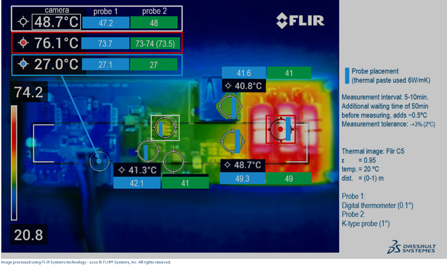
Measurement setup
The measurement is performed with help from thermal imaging (a thermal camera) and two probes (a K-type thermocouple probe and an indoor thermometer) in order to validate the read-out. Utilization of the probes is essential to obtain and determine an accurate value of tested device emissivity and ambient temperature for thermal imaging purposes. Based on the acquired temperature values, an average temperature is calculated for all measuring points. The probe locations are shown in Fig.5.
Remark 3: Conducted tests do not classify as a certified type of measurement.
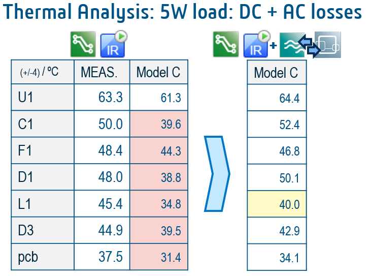
Based on measurement tolerances and the simulation of a simplified thermal model, an assumption is made to estimate a maximum deviation between simulation and measurement results at the level of +/- 4°C. All compared temperatures are listed in the following tables (Fig.6 and Fig.7). If a simulated temperature exceeds the limit, the corresponding field in the table will be marked in orange.
Simulation of the model A and B indicates that the complexity level of CAD shapes should always be considered depending on user needs. As Fig.6a depicts, model B runs almost 4x faster than model A while overall temperature deviations between them are not significant. The use of simplified CAD shapes allows the user to perform more simulation experiments and learn more about the device behavior in different scenarios, which is almost always appreciated, especially during the design stage.
Fig.6 (6a, 6b) shows that depending on device loading conditions, the accuracy of the simulation can decrease.
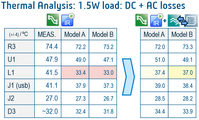
It is important to remember that CST Studio Suite workflow performs an IR-Drop analysis in order to compute input parameters (data) required by the thermal solver. The IR-Drop analysis obtains power losses of the PCB only at the DC level, based on calculated voltages and currents of a circuitry. Therefore no AC power losses are taken into account. To consider these, a 3D co-simulation can be performed in CST Studio Suite.
The analyzed device belongs to the family of SMPS (switched-mode power supply), which means that because of the switching mechanism used by the device to control its output voltage/current levels, a part of the power transfer occurs via harmonics generated by a switch. How big this part is depends not only on the switching topology but also on the loading conditions.
Fortunately, in CST Studio Suite a user can very quickly generate a 3D model of the previously imported PCB, and together with the integrated circuit simulator run a so-called 3D co-simulation, which will compute additional AC losses of the layout and on-board components.
This approach comes in handy for any PCB components in which AC losses are dominant.
For example:
- power inductors, transformers, chokes and other related components which experience power losses due to core losses, AC and DC resistance losses of the windings;
- switches (IGBTs, MOSFET transistors) in which losses come from conduction, switching mechanism and gate charge losses.
Agreement between measurement and simulation
Applying a co-simulation to the analyzed PCB leads to the results shown in Fig.7, with agreement between measurement and simulation results is reached. The temperature of the system inductor (L1) slightly exceeds the maximum tolerance, mainly because of the unknown material used for its core.
A thermal simulation of a PCB using the IR-Drop solver is relatively quick to set up and run.
All simulated cases were run on a laptop equipped with a four-core Intel® i7-6820hq® processor.
The accuracy of computed results depends on the character of the losses present in the analyzed system. If AC losses are dominant, it is recommended to run a 3D co-simulation in order to accurately capture them and add these into the thermal analysis.
Summary
The agreement between the measurement and simulation shows that the IR-Drop and CFD workflow is an effective way to calculate heating due to electrical losses in PCBs. The workflows demonstrated in this blog post are easy to set up from standard EDA layout files, and can run on local resources such as a single laptop. CST Studio Suite offers a powerful tool for electronics engineers to use to quickly assess the thermal performance of their designs without a physical test board.
Want to learn more about CST Studio Suite and connect with other CST Studio Suite users? Visit our SIMULIA Community to discover the latest tips, to ask questions and to share your expertise. Our dedicated CST Studio Suite Learning Resources page is a great place to start exploring.
SIMULIA offers an advanced simulation product portfolio, including Abaqus, Isight, fe-safe, Tosca, Simpoe-Mold, SIMPACK, CST Studio Suite, XFlow, PowerFLOW and more. The SIMULIA Community is the place to find the latest resources for SIMULIA software and to collaborate with other users. The key that unlocks the door of innovative thinking and knowledge building, the SIMULIA Community provides you with the tools you need to expand your knowledge, whenever and wherever.

Marcel is a solution consultant for electromagnetic simulation at Dassault Systèmes in Darmstadt, Germany. In 2011, he received the M.Sc. degree in microwave and RF specialization from the Silesian University of Technology in Gliwice, Poland. He was engaged in consumer electronics market as a hardware engineer until 2014. He then joined CST as an application engineer. He is active in the simulation of SI, PI and EMC and also in the design of electronics.