By Dr. Hany Fahmy, a Technologist of Signal Integrity and Electromagnetic Compatibility.
Introduction
Moore’s Law, the famous statement underpinning the semiconductor industry, predicts that the density of transistors on a chip will double every two years. In recent years however, Moore’s Law has slowed down as chip manufacturers approach fundamental physical limits and the cost of developing new technology increases rapidly. Instead, chipmakers are looking for other ways to increase chip performance.
One promising approach is heterogeneous integration. Rather than implementing all functions on a monolithic silicon wafer, heterogeneous integration packages different functions onto different chiplets, using the most appropriate and cost-effective manufacturing node for each, and integrates them in a system-on-chip (SOC). Modular chiplets can be combined in different ways, mixing and matching them to meet the needs of the application. Compared to monolithic approaches, heterogeneous integration reduces costs and allows manufacturers to keep pushing the limits of performance.
To connect the chiplets, a high-parallel bus interface with source synchronous architecture is often used. This is an effective way to reduce latency and maintain a high bandwidth. However, implementing this introduces its own challenges.
This blog post gives an overview of how simulation can be used to analyze and optimize chiplet interconnects with source synchronous architecture, to help engineers design cutting-edge SOCs. This is based on a paper originally presented at DesignCon 2023, which can be read in full on the SIMULIA Community.
Challenges of Chiplet Architecture
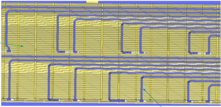
The disaggregated nature of a SOC designed with heterogeneous integration means that there are many separate chiplets that all need to be connected. If the latency of this connection is too high, the performance advantage will be lost.
To achieve low transmit latency, a parallel bus with source synchronous architecture is commonly used, such as in HBM and UCIe standards. In a source synchronous architecture, a clock (strobe) is transmitted on dedicated traces along with the data. Because flight time can vary across different traces, to have all the data signals correctly sampled by the strobe, data signals must to be matched out of phase – in other words, in skew.
The requirement of matching the skew of data and strobe traces is critical in chiplet channel implementation. To preserve this phase relationship, the data and strobe need to be matched to each other as close as possible based on their propagation delay.
3D Full-wave Simulation of Source Synchronous Architecture
Traditional 2D circuit extraction simulation methods fail to provide accurate results for SOCs, because it does not capture the high-density vertical coupling among tightly packed channels, nor the effects of conductor thickness and resistivity. This is an even larger problem when data rates can be measured in GHz, as even very slight timing mismatches are enough to cause error.
3D structures such as silicon interposers and through-silicon vias (TSV) and meshed ground planes also need to be taken into account. On a silicon interposer, technology rule requirements mandate the use of meshed ground planes. This means that although two signal traces may have the same length, the return current can have very different routes and therefore the total flight time can vary significantly.
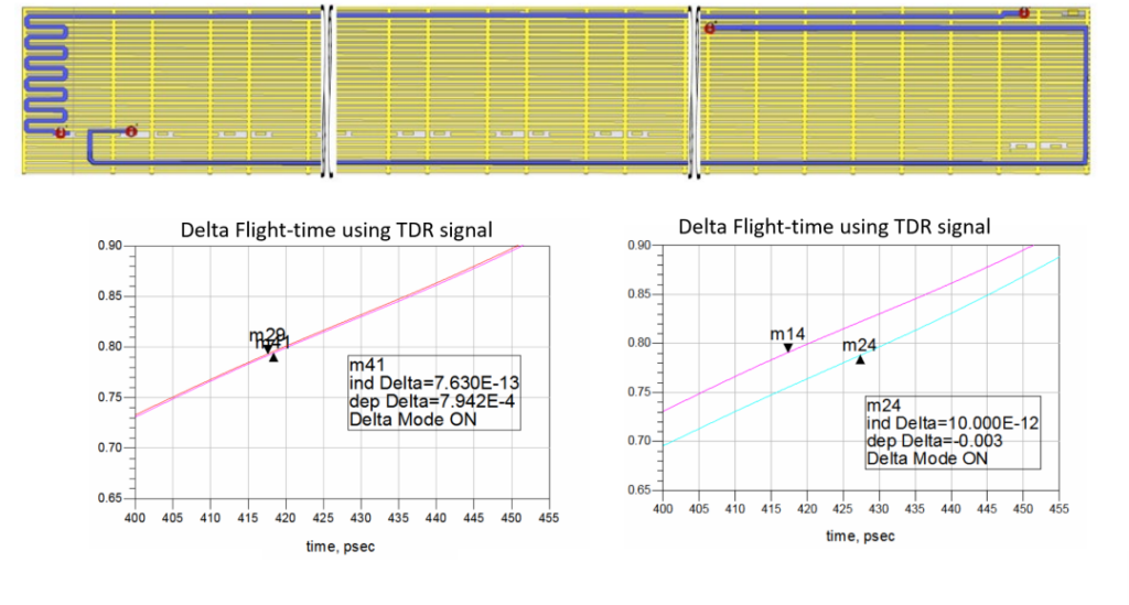
Comparison of 2D to 3D Simulation
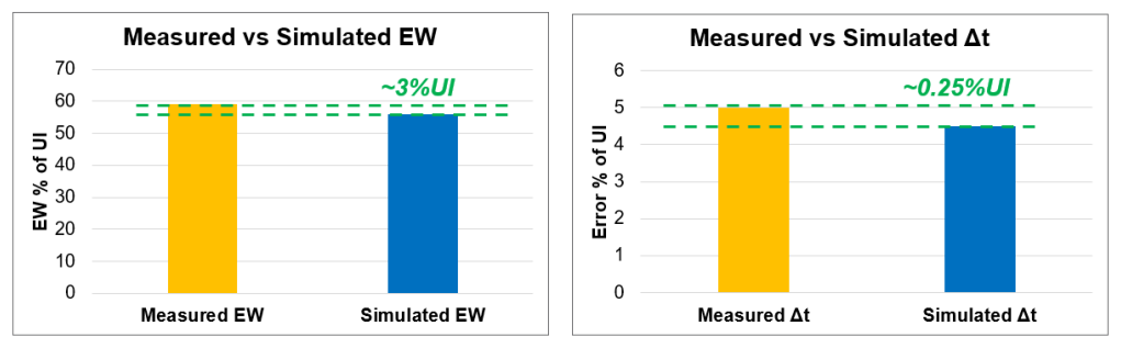
The simulation in Figure 2 shows the impact of choosing 2D vs 3D simulation. On the same structure, a 2D simulation found an estimated delay skew under 1 ps, while a 3D simulation calculated the delay skew at 10 ps. The 2D simulation missed significant contributions from the circuit geometry, which resulted in a ten-fold increase in delay skew. On a 10 Gbps data channel, this would equate to a 10% error rate. Accurate simulation is therefore critical. With 3D simulation using SIMULIA CST Studio Suite, excellent agreement between simulation and measurement can be achieved, giving engineers confidence in the simulation (Figure 3).
Learn More about Source Synchronous Architecture Simulation
This blog post has only scratched the surface of simulation for SOCs. A full workflow, demonstrating both simulation and measurement as well as the fundamentals of source synchronous architecture design, can be found in our paper 3D EM Full Wave Analysis & Optimization for Source Synchronous Interconnect in Heterogeneous Integration Architecture. This paper, presented at DesignCon 2023, can be read on the SIMULIA Community.

This post was authored by Dr. Hany Fahmy a Technologist of Signal Integrity and Electromagnetic Compatibility with 25-years’ experience in the design and analysis of High-Speed Digital and Analog interconnects: Memory, Ethernet Backplanes, PCI-e, DVI/HDMI/LVDS/DP and USB. Hany worked at Nvidia as the director of SI/PI/EMC group designing Smartphones/Tablets and GPU-cards: chartered to simulate, model and lab characterize advanced high speed digital solutions. He was the leader of the Memory Architecture Group at Intel Corporation with expertise in designing desktop, mobile and server platforms for complex CPU/GPU’s and chipsets. Hany represented Intel in JEDEC as the memory architect for DDR1/2/3 technology development. He also worked at Micron and Agilent Technologies along with Texas Instruments Inc. Hany is the author of eleven-patents, and he is now leading Intelligent Solutions BVBA as the CEO & Chief Consultant Officer. Hany is a consultant in AMD system IO Platform team.

Interested in the latest in simulation? Looking for advice and best practices? Want to discuss simulation with fellow users and Dassault Systèmes experts? The SIMULIA Community is the place to find the latest resources for SIMULIA software and to collaborate with other users. The key that unlocks the door of innovative thinking and knowledge building, the SIMULIA Community provides you with the tools you need to expand your knowledge, whenever and wherever.

Katie is the Editor of the SIMULIA blog, an expert in engineering and scientific communication, and a strategic digital marketer. Katie has a BA in English and Writing from the University of Rhode Island and a MS in Technical Communication from Northeastern University. She is also a proud SIMULIA advocate, passionate about democratizing simulation for all audiences. Katie is a native Rhode Islander who lives just outside of her favorite city, Providence. She is a true New Englander and loves sharing all the cool things NE has to offer. She enjoys a variety of hobbies including history, astronomy, science/technology, science fiction, true crime, fashion and anything associated with nature and the outdoors. She is also mom to a 6-year old budding engineer and two crazy rescue pups.