
Background
Data hungry applications such as high-definition streaming video, gaming and smart devices – as well as industrial applications such as telemedicine and autonomous driving – require both higher bandwidths and reliable connections.
To support higher data rates, signal pulses must switch on and off faster – in other words their rise and fall times decrease. Signal integrity is harder to achieve with higher signal bandwidth and shorter rise times, especially in structures like connectors, due to problems such as reflections from discontinuities, material losses, crosstalk from other channels, and mode conversion from asymmetries.
Electronic data channels need to facilitate data transfer with minimal distortion of the signal. PCBs, connectors and cables that transmit the signals may act as a source of unwanted noise, potentially interfering with nearby electronics. Hence, it is extremely important to ensure high signal integrity and to meet electromagnetic compatibility (EMC) certification standards.
The connection also needs to be reliable not just on the first use, but on the hundredth or the thousandth. The pins have to make contact correctly in order to minimize the reflection and loss that can cause signal integrity problems, and the springs need to hold the connector in place with the correct force, so it does not come out accidentally but still can be inserted and removed easily by the user.
Devices are evolving rapidly and so have a very short product life cycle that limits the available time for design and analysis. Given such short time frames, how do we improve prediction capabilities and make better design decisions?
What is MODSIM?
Computer aided design (CAD) modeling and Computer Aided Engineering (CAE) simulation are both well established. MODSIM – an abbreviation of “Unified Modeling and Simulation” – combines these, integrating CAD with simulation tools on one common database to analyze the performance of the device during the design process. All model and simulation data is stored in a single source of truth, so all users are working with the same, up-to-date information. The CAD model is used directly to construct the simulation model, and the simulation results in turn are used to guide the design.
MODSIM accelerates development because it allows designers to verify that the product meets the specifications and requirements from the earliest stages of design, rather than committing resources to developing and prototyping an idea only to discover a problem during testing.
In the case of a connector, MODSIM offers several benefits:
- Reduce the number of prototypes needed: As potential issues can be identified without physical testing, physical prototypes only need to be manufactured when the designer is confident that the design meets SI and EMC requirements.
- Improved communication between departments: Design and simulation traditionally work in silos. By integrating the two, MODSIM enables collaboration, giving designers more direct access to simulation data.
- Accelerate development: MODSIM also speeds up development because CAD models can be transferred directly to simulation, reducing the work needed to prepare a simulation-ready model for all the different types of simulation. The simulation results can then in turn be used to improve the design – or even to optimize it directly with automatic parametric or non-parametric optimization.
MODSIM workflow for a USB connector
Phase 1: Define requirements
In the first phase of the project, the product owner and the CAE manager create a comprehensive list of requirements for the connector project. These requirements ensure that the connector will satisfy both electromagnetic and structural specifications and comply with industry standards. Requirements might include:
- Insertion and removal force (upper and lower limits)
- Fatigue and insertion cycles
- Signal integrity
- Legal EMC limits
- Geometric limitations (size, shape)
The Requirement app (from the ENOVIA brand of Dassault Systèmes) is used to create project and design related requirements. These are structured in different classes, giving full overview of all KPIs. For example, there are radiated emission (RE) requirements under the EMC specification folder, following FCC standards for different frequency ranges. The users can add requirement details under requirement specifications, which contain various parameter values or ranges of parameters, their priority and maturity status, the owner of the requirement and so on.
At this stage, the tests needed to verify compliance with the requirements can also be defined in the ENOVIA Test Management app, and assigned to the responsible engineers.
Phase 2: Modeling
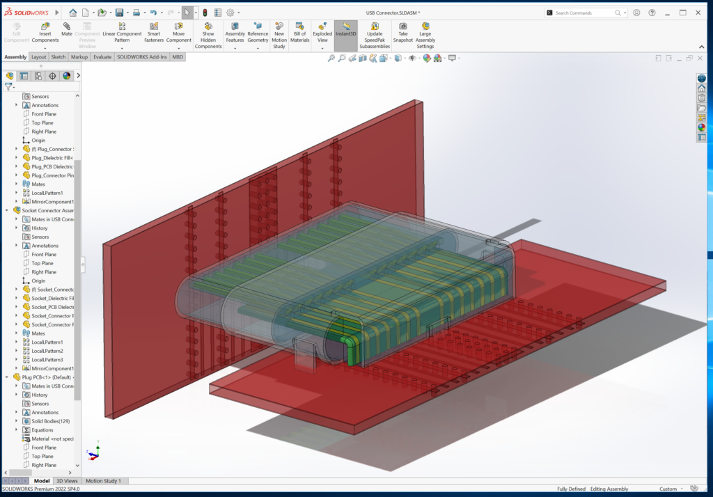
The design expert and the SI engineer, responsible for the simulation, will work together to assure the connector is meeting SI requirements. A parametric model is created using SOLIDWORKS connected and simulated on cloud.
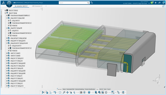
Figure 2 shows the connector model designed in SOLIDWORKS. It consists of the male and female parts, each connected to their respective PCB. The model is parametric which simplifies the process of making changes to the geometry and design exploration. This model is saved to the 3DEXPERIENCE platform so that it can be accessed by all the stakeholders involved in the project.
Phase 3: Simulation
Now the SI engineer launches the electromagnetic simulation tool CST Studio Suite in Power’By mode and receives the updated model from the 3DEXPERIENCE platform. The model is saved locally with simulation settings, so important aspects such as frequency range, meshing, ports and excitation signals are defined, after which the simulation can be executed locally or on the 3DEXPERIENCE Cloud platform. The 3DEXPERIENCE Cloud platform brings the power of high-performance computing (HPC) to users with occasional demanding simulation needs, for whom dedicated on-site hardware would be too expensive. The cloud democratizes simulation, allowing designers to make better use of it and improve the MODSIM workflow.
A special electromagnetic solver is used called “Transient Transmission Line Matrix (TLM)”, which is well-suited to simulating interference/EMC on complex geometry. It uses the Perfect Boundary Approximation (cell warping) and cell lumping to significantly reduce the number of cells required to mesh the geometry, without jeopardizing the simulation’s accuracy. If necessary, the simulation can also include the cable itself and the geometry of the entire phone.
At the same time as the electromagnetic simulation, the mechanical performance of the connector can be simulated. Using the 3DEXPERIENCE platform, the connector model is opened in Abaqus, the structural simulation tool from SIMULIA. The insertion process is simulated using a “Virtual Twin” of the connector, outputting results such as strain on the pins (and resulting deformation), holding force and fatigue over many cycles.
Stage 4: Analysis
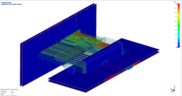
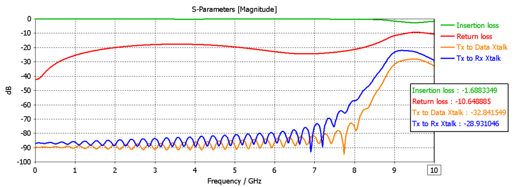
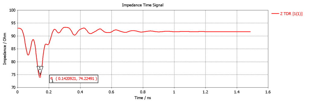
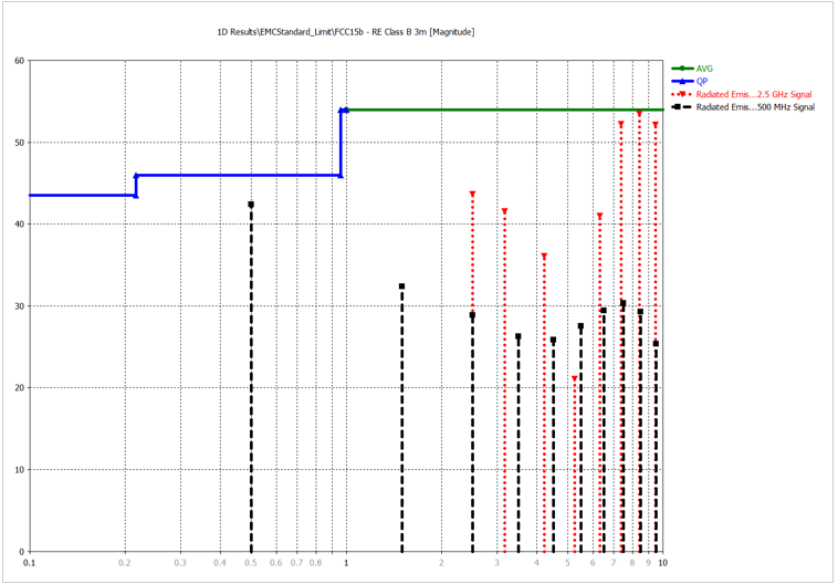
Figure 3 shows the simulated model of the connector and the ports that have been excited using differential signaling. Figure 4 displays a frequency plot of the return loss, the insertion loss and crosstalk signals and Figure 5 the Time Domain Reflectometry (TDR) signal. The user can visualize and animate the surface current distribution over the high-speed connector. EMC compliance can be analyzed with virtual probes that capture the E-field at a distance of 3 meters in different directions. These reflect the FCC standards for Radiated Emissions Class B. Figure 6 shows the peak emissions for a 500 MHz USB signal and for a high-speed 2.5GHz USB signal.
The 3DEXPERIENCE platform offers a summary of the results. In this example, crosstalk is well within limits at all the frequencies, indicating that the crosstalk requirements have been met. The same is true for Insertion loss, but when it comes to TDR, the differential TDR impedance is lower than the required value. Likewise, the return loss at 10 GHz is slightly higher than the maximum allowable value. Therefore, we can say that the current design does not meet the impedance and return loss requirements. In order to rectify this, a design change is required.
Stage 5: Remodeling and change management
The signal integrity engineer identified that the baseline TDR showed too much of a dip in impedance at the spring location, and opted to reduce the length of socket pin stubs which may have been adding parasitic capacitance. This design change has to be communicated with the design expert. They will work together using Change Management to ensure the necessary changes to the connector model so that it meets the SI requirements and also complies with EMC standards, to be checked by the EMC engineer.
To request the change, the SI engineer uses Issue Management. The issue will be attached to the baseline geometry and will be visualized with a placemark. The designer is asked to modify the pin length of the socket in SOLIDWORKS. Once the value of the respective variables has been modified in SOLIDWORKS, the updated model will again be saved on the platform as a revision. The new design can be re-simulated – with both electromagnetic simulation and structural simulation – to ensure that it now meets the requirements and does not compromise mechanical performance. The simulations confirm that compliance with electromagnetic requirements does not adversely affect the electromagnetic performance of the connector.
This model will be placed under the resolve tab of the issue management so that the owner will be notified that the model has been updated. They can check the changes and send it for approval.
Stage 6: Approval
Once the issue has been resolved, and the design now meets TDR requirements as seen in the graph, the SI engineer can update the new test results under Test Management by verifying the new results and this test case can be marked as passed. So the update will go to the project manager and after reviewing the results, the test is marked as passed and sent for approval to the CAE manager. The CAE manager can approve the test and can release the requirement.
Conclusion
The MODSIM workflow significantly accelerates development compared to a conventional design flow, where the TDR issue would likely only have been detected after completing the design and constructing the prototype. All tools – requirements management from ENOVIA, modeling with SOLIDWORKS and simulation with SIMULIA – were available from the 3DEXPERIENCE platform. The team was able to work together on the 3DEXPERIENCE platform, sharing an automatically-updated common model to ensure all are working with the latest data. The end result was a connector that met all electronic certification requirements and standards.

Interested in the latest in simulation? Looking for advice and best practices? Want to discuss simulation with fellow users and Dassault Systèmes experts? The SIMULIA Community is the place to find the latest resources for SIMULIA software and to collaborate with other users. The key that unlocks the door of innovative thinking and knowledge building, the SIMULIA Community provides you with the tools you need to expand your knowledge, whenever and wherever.

Stephen is an Advocacy Offer Marketing Specialist in Global Marketing.