Executive Summary
A quantum bit (qubit) is the fundamental unit of information used in a world of quantum computing. Instead of having two distinct states, bit 0 and bit 1 as in classical computing, a qubit can exist in a linear combination of both states simultaneously (superposition), and it can be linked in such a way that the state of one instantly influences the state of another (entanglement). Because of these two key properties of a qubit, a computer’s processing power can be increased exponentially. The physical implementation of a qubit can be either using photons, trapped ions (a single charged atom that is held in place using electromagnetic fields) or superconducting circuits. The latter is the most mature and widely used technology since it can be built on the existing semiconductor manufacturing techniques.
Transmom Qubit Circuit
In one qubit system, the integrated circuit of transmon qubit circuit consists typically of four components:
- Feedline
- Resonator
- Transmon qubit with one Josephson Junction (JJ)
- Current bias line
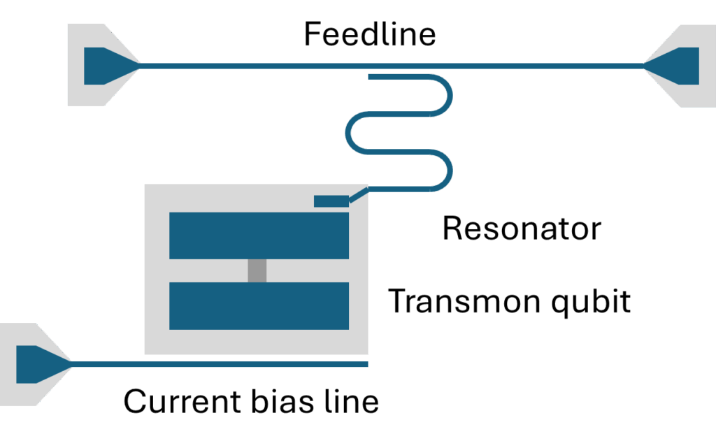
The transmon qubit in this case consists of one Josephson junction (jj). It is located at the center of the transmon qubit and connected with the two metal pads. Josephson junction is the key part of the superconducting qubit. The Josephson junction structure consists of two superconductors separated by a thin insulation barrier. The superconductor is usually made of aluminum (Al) and becomes superconducting below 1.2 K. While a normal inductor has a constant inductance value, the jj is non-linear. The value increases or decreases as we add energy. The resonator and feedline are made of a coplanar waveguide (CPW) structure with an atypical 50 ohm characteristic impedance. The resonator and feedline are used to measure the state of qubit. The change in the Josephson junction inductance can be measured by creating a tiny magnetic field from the current bias line.
Superconducting Qubit Chip Assembly
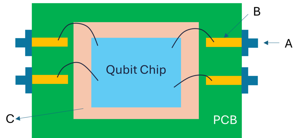
The transmon qubit circuits are integrated into one chip and then connected with the PCB to allow measurement or qubit manipulation. Figure 2 shows the simplified diagram of a typical superconducting qubit chip assembly. The qubit chip is mounted at the center of the PCB within a recessed cavity (C). To enable the qubit manipulation and readout, a wire bond connects the chip to the PCB traces (B) and routes the microwave signals to the edge-mounted SMA connector (A). Through these SMA connectors, high-frequency signals are transferred to and from the measurement device. The PCB size is in the millimeter range, while the qubit chip is in the sub-millimeter range. The entire assembly is cooled in a dilution refrigerator close to absolute zero, at several 10 mK. At this temperature, the electronic circuits made from superconductors such as aluminum or niobium flow without resistance, allowing them to behave like artificial atoms that serve as qubits.
Superconducting Material Definition
In the 3D EM simulation, the superconducting material can be defined in two ways. The simplest method is to define a loss-free material, such as a PEC (Perfect Electric Conductor) or a loss-free normal material, for example, a substrate. This method is sufficient to get the design resonance frequency. However, for an accurate Q-factor calculation, the loss-free material definition is not recommended, as it yields a Q-factor that is too high. Thus, using a lossy material yields a more accurate Q-factor value, but requires slightly more computational resources. In CST Studio Suite, the superconducting material property is defined using surface impedance modeling. This approach is valid because the thickness of the superconductor is usually several micrometers. The superconducting material definition can be found in: VBA macros–>materials–>Tabulated surface impedance (broadband) as seen in Figure 3.
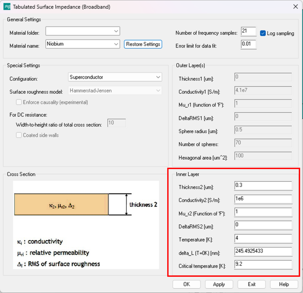
The material properties, such as conductivity at room temperature, superconducting working temperature, London penetration depth and critical temperature, are to be defined to calculate the surface impedance ▁Z. For the substrate material, silicon with Epsr=11.9 is defined with very low loss, TanD=1e-6. More details about this superconducting material definition in CST can be found in [4].
Design Parameter
Most quantum measurement hardware is optimized for frequencies between 4 GHz and 8 GHz. Therefore, the transmon qubit frequency is 5GHz. To avoid interference with the qubit, the resonator frequency is set to 7 GHz. According to [1], to have a well-behaved transmon qubit, additional constraints need to be met, such as
|α| > 200 MHz (1)
E_j/E_c >50 (2)
α is anharmonicity, and larger anharmonicity helps to isolate the |0⟩ and |1⟩ from higher energy levels, while the ratio E_j/E_c needs to be large enough so that it is insensitive to the charge noise. The Josephson junction energy (Ej) and the charging energy (Ec) can both be expressed in MHz as follows:
Ec= e^2/(2∙C∙h)∙10^(-6)
(3)
Ej= 〖Φ_0〗^2/((2π)^2∙L_j∙h)∙10^(-6)
(4)
With e = 1.602∙10^(-19) coulombs, Φ_0 is superconducting flux quantum (~ 2.067∙10^(-15) Wb) and h is Planck’s constant (~ 6.626∙10^(-34) Js). As we need to satisfy equation (2), the anharmonicity and charging energy can be approximated as
α= -E_c (5)
Transmon Qubit Capacitance
To calculate the charging energy Ec from (3), we need to determine the transmon qubit’s capacitance C. The capacitance of the transmon qubit is calculated using the E-static solver. The size of the transmon qubit is shown in Figure 4. The metalization thickness is 20um.
Using the E-static solver, the capacitance value C= 93.5fF is calculated based on the pad size 500um x 200um. Inserting the capacitance value into equation (3), we obtain the charging energy Ec = 207 MHz. In practice, the Josephson junction inductance Lj is typically between 1nH and 20nH. In this case, the Josephson junction inductance Lj = 10 nH is defined. With (4), the Ej is 16333MHz. The ratio E_j/E_c is approximately 78.87. With (5), the anharmonicity is -207 MHz; thus, the design constraints are fulfilled.
Box Mode Calculation
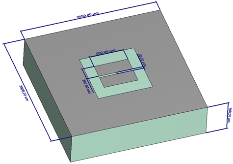
In practice, the transmon qubit chip is placed inside a metallic box to isolate it from environmental noise. The lowest box mode cavity resonance shall be larger than the transmon qubit and resonator resonance to prevent energy coupling between the qubit or resonator and the box. The lowest box mode cavity can be obtained easily using the eigenmode solver or the analytical formulation of a rectangular waveguide [2] given by
f_mnl= c_0/(2π√(ε_r )) √((mπ/a)^2+(nπ/b)^2+(lπ/c)^2 )
(6)
Given the size of the qubit chip (2758um x 3000um x 1500um), the lowest box mode is at 73.82GHz. Since the lowest box mode frequency is much higher than the resonance frequency of the transmon qubit and resonator, we don’t need to worry about the interaction between the box mode and qubit. In addition, it allows us to choose close boundary condition (Et=0) for the simulation using the eigenmode solver and frequency domain solver.
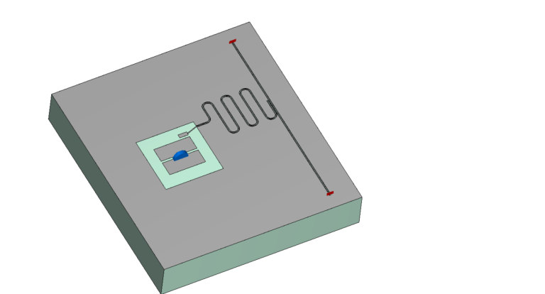
Transmon Qubit, Resonator and Feedline
To simulate the transmon qubit and resonator frequency, the eigenmode solver is used here. The Josephson junction cannot be simulated with a 3D solver. To consider the effect of the Josephson junction, a lumped element with inductor value Lj =10nH is used and connected between two conductor pads. The readout path is composed of a resonator and a feedline. Both are coplanar waveguides (CPWs) with a 10 um signal width and a 6 um gap between the signal line and the ground plane. This gives the characteristic line impedance of 50 ohms.
The resonator design is a quarter-wavelength (λ/4) resonator. An open-end resonator capacitively couples to the transmon qubit, and the other end is shorted to GND. This shorted end is then coupled inductively to the feedline. Thus, at this end, the voltage is almost zero and the current is maximum. The complete model of the transmon qubit, resonator and feedline is shown in Figure 5.
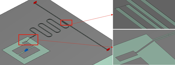
At both ends of the feedline, the waveguide ports are configured to terminate it. Using the waveguide ports, the eigenmode solver can also calculate the Qext value. This Qext value indicates how well the qubit is protected from the outside world. The eigenmode solver also provides the Qtotal, which includes all internal losses.
Using the Qtotal of the qubit, we can estimate the qubit relaxation time (T1)
T_1=Q_total/f_q (7)
And using the Qext of the resonator, we can estimate the readout time (Tr).
T_r=Q_ext/f_r (8)
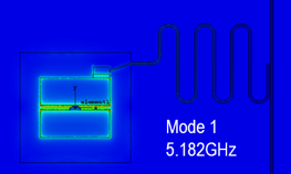
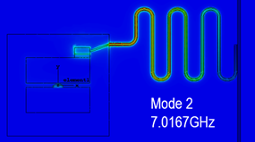
Eigenmode Solver Simulation Results
The frequency range for the eigenmode solver is 4 GHz to 8 GHz. It is configured to support two calculation modes. The e-field distribution for modes 1 and 2 is shown in Figures 6 and 7. The field distribution at mode 1 is concentrated at the transmon qubit with a frequency of 5.18 GHz, and the second mode frequency is 7.017GHz. The field distribution at the second mode concentrates on the resonator. The Qtotal value from mode 1 is approximated at 1.27e6. This is a good indicator that the qubit is well isolated from the feedline and not coupled to it. If we consider this Q value in equation (7), we get an energy relaxation time of 245.3us. The simulated Qext value from mode 2 is 15839. Using equation (8), we obtain a readout time of 2.25 us. A reading pulse of hundreds of nanoseconds can be used to read out the qubit. This is faster than the qubit’s decoherence time. Which is according to [1] about 50us-200us.
Frequency Domain Solver Simulation
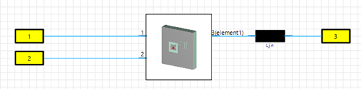
To simulate the inductance change of the Josephson junction, the frequency-domain solver has been used. Due to the structure’s high Q-value, it is highly recommended to use the FROM (Fast Reduced Order Model) solver. The lumped element is replaced with the discrete face port, and the fd-solver simulation runs all port definitions to create a full S-matrix. The so-called EM-circuit coupled simulation method is used, in which the inductor connection is implemented within the circuit simulator, CST Design Studio. This method gives a more efficient simulation, as circuit simulation runs faster than a full 3D simulation. Figure 8 shows the transmon qubit model, where port 3 is defined to replace the lumped element. The corresponding circuit schematic connection realized in CST Design Studio is shown in Figure 9. Port 1 and Port 2 are terminated with 50 ohms, and Port 3 represents the internal localized junction port, which is terminated with 1e-5 ohms, indicating a parasitic impedance of almost zero for the inductor.
By sweeping the inductance value Lj of 10nH, 11nH and 12nH, we could obtain the frequency shift at the resonator by looking at the S1,3 results. The three curves are shown in Figure 10.
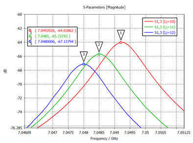
A change in inductance shifts the resonator frequency, a phenomenon called Cross-Kerr (χ). 2χ is similar to full width at half maximum (FWHM), Δf. The Δf can be read out from the S1,3 curve at maximum, which is around 500kHz-700kHz. Cross-Kerr (χ) is given with the following equation,
χ≈g^2/∆ (α/(∆+α))
(9)
The detuning (∆) is defined as the resonance frequency difference between the transmon qubit (mode 1) and the resonator (mode 2) and is given as follows,
∆ = f_resonator-f_qubit (10)
Using a Δf of 700kHz, the coupling strength g can be calculated from (9) to be ~ 72.8 MHz. A coupling strength smaller than the detuning (∆) is a good choice, as it can provide a good readout. Another alternative for calculating the cross-Kerr is to use the energy participation ratio (EPR), as described in [3].
Conclusion
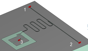
Using the 3D EM simulation tool helps engineers accelerate and precisely design the transmon qubit, resonator and feedline. The Estatic solver is used to calculate the transmon qubit’s capacitance. The eigenmode solver is useful for mode frequency calculation of the transmon qubit and resonator, while the frequency domain solver is very efficient to simulate the Cross Kerr (χ) effect by sweeping the Josephson junction inductance Lj. In addition, this blog article shows the benefits of using simulation tools to design the qubit readout flex PCB, which transfers the signal from the qubit chip to the main computer.
References
[1] Hiu Yung Wong, Quantum Computing Architecture and Hardware for Engineers
[2] David M. Pozar, Microwave Engineering
[3] Quantum Metall (https://qiskit-community.github.io/qiskit-metal/)
[4] CST Studio Suite® 2026 Online Help

Interested in the latest in simulation? Looking for advice and best practices? Want to discuss simulation with fellow users and Dassault Systèmes experts? The SIMULIA Community is the place to find the latest resources for SIMULIA software and to collaborate with other users. The key that unlocks the door of innovative thinking and knowledge building, the SIMULIA Community provides you with the tools you need to expand your knowledge, whenever and wherever.

Richard Sjiariel joined Dassault Systemes Deutschland since June 2021. His current position is SIMULIA Industry Process Consultant with the main focus of EMC simulation. From 2015 to May 2021, he was a hardware developer at Continental Automotive GmbH, Germany, where he was responsible for automotive display development, such as power supply concept, FR4-PCB and Flex-PCB layout architect, signal- and power integrity simulation and measurement, as well as EMC measurement according to CISPR-25. Before joining Continental, he was working 8 years as application engineer at CST. He gave technical support, training and webinar with the application area signal integrity and power integrity. He finished his M.Sc. degrees in electrical engineering from University of Wuppertal in 2006.