This article was originally published in the June 2018 issue of SIMULIA Community News magazine and is authored by Pierre Wahl, co-Founder of Luceda Photonics.

The use and manipulation of light has always been a key component in technological fields such as telecommunications, medicine, sensing and defense. The science behind the manipulation of light is broadly known as “optics” or “photonics.” Over the last decade the possibility of integrating photonic capability on a chip has started an unprecedented wave of innovation in the optics community such that it became a field of its own: “Integrated photonics.” Already today, the use of integrated photonics has enabled order of magnitude improvements in the cost, performance and energy consumption of telecommunication while other fields are catching up quickly. Having supported R&D teams of major corporations and research institutes all over the world, we advise the following to teams hoping to reap similar benefits of this exciting technology.
CONSIDER ALL THE COSTS AND BENEFITS FOR YOUR APPLICATION
While the use of integrated photonic systems almost always improves the performance of their non-integrated counterparts, an integrated photonic chip is always part of a broader system in which it has to be integrated. As integrated photonic chips have different R&D processes, production facilities and cost models than their bulk counterparts, one needs to carefully consider both the technological and economic implications of the switch. For instance, it is true that integrated chips can have a very low unit cost but that is only the case when you need a large number of them. Sweat the details about this before you start making major financial commitments.
PROCESS DESIGN KITS (PDKS) AND MULTI PROJECT WAFERS (MPWS)
To help lower the adoption risk of industrial players, the research foundries active in integrated photonics offer you the possibility to share the cost of a full development wafer among different participants by combining their designs onto a single wafer. On top of that most foundries provide process design kits or PDKs that contain tested building blocks you can easily assemble and reuse. We therefore strongly recommend recent adopters to fully utilize this option to benchmark the technology.
INVEST IN A ROBUST WORKFLOW
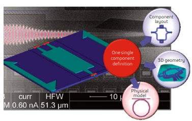
Electromagnetic field simulations are a very important aspect of integrated photonics design. Nevertheless, we see that in practice, photonics design teams struggle with the organizational aspects required to consistently configure such simulations properly. It is necessary that the simulated geometry is a correct representation of the final fabricated structure, that the material models used are correct under operating conditions and that the simulation settings are set sensibly to obtain an accurate result in a reasonable time. Often, designers have to consult a range of sources and people (PDK handbook, process information data and the expertise of an engineer specializing in simulations) to get their simulation configured properly. As those sources are continuously updated, ensuring that your EM simulations are consistently correct is mostly an organizational challenge. The use of software that can handle all aspect of the design flow is very important. At Luceda we collaborate with Dassault Systèmes to bring the best possible flow to our shared customers.
ABOUT THE AUTHOR
Pierre Wahl co-founded Luceda Photonics in 2014 where he is in charge of sales, support and training operations. At Luceda he trains and supports R&D teams of major corporations, research institutes, foundries and universities in China, North America and Europe.
He completed a PhD in opto-electronics at the Free University of Brussels and Stanford University on ultra-low energy optical interconnects in 2014 and obtained a Masters degree in photonics from the University of Gent and the Free University of Brussels in 2010. He has co-authored multiple journal publications and delivered various talks around specialized design, simulation and optimization techniques used in integrated photonics.
ABOUT LUCEDA PHOTONICS
Luceda Photonics wants photonic IC engineers to enjoy the same first-time-right design experience as electronic IC designers. Luceda Photonics’ tools and services are rooted in over 50 years of experience in photonic integrated circuit (PIC) design and are used by several research institutes and industrial R&D teams worldwide.
For More Information: www.lucedaphotonics.com

Martin is the Marketing Director for SIMULIA EMAG, in Global Marketing.