
This article shows how the simulation of the DCDC converter with CST Studio Suite® can be used to predict the electromagnetic compatibility (EMC) performance. By considering the spread spectrum clock generation and an EMI receiver in the simulation, more realistic results can be achieved.
Background
DCDC converters, as the name implies, are a group of electronic systems that are used to convert the DC voltage to the different required levels. DCDC converters can be found in almost all electronic products. For converting DC power with a high efficiency, the switch-mode power supply (SMPS) concept is used. However, the SMPS could raise an issue in electromagnetic compatibility (EMC) if the design process is not EMC-aware. Both conducted emission (CE) and radiated emission (RE) mitigation needs to be included in the design process.
For the conducted emission, the high-frequency noise created by switching is coupled to the main power supply and measured, depending on the EMC standard, from several kHz up to several hundred of MHz. For example, the CE measurement frequency range according to CISPR-25, an automotive EMC standard, is between 150 kHz and 108 MHz. For radiated emission, the emission from the PCB is picked up by the receiver antenna typically placed at a 3m distance.
The radiation of the SMPS would not only come from noise that coupled to the power line cable but also from the poor PCB layout routing, which creates a non-optimum switching node loop. The RE measurement frequency range starts usually from 30 MHz up to several GHz. Generally, in order to reduce the noise and comply with EMC standards, the layout and/or the filtering components need to be optimized.
An alternative technique to reduce emitted noise levels is discussed in this article: the spread spectrum clock generation (SSCG) technique. It has been widely used in power electronic applications, especially for DCDC converters. Applying this technique doesn’t require any component or layout modifications. We just need to make sure that the regulator driver supports this technique.
Circuit Simulation of DCDC Converter
The below picture shows the typical circuit of a DCDC boost asynchronous converter.
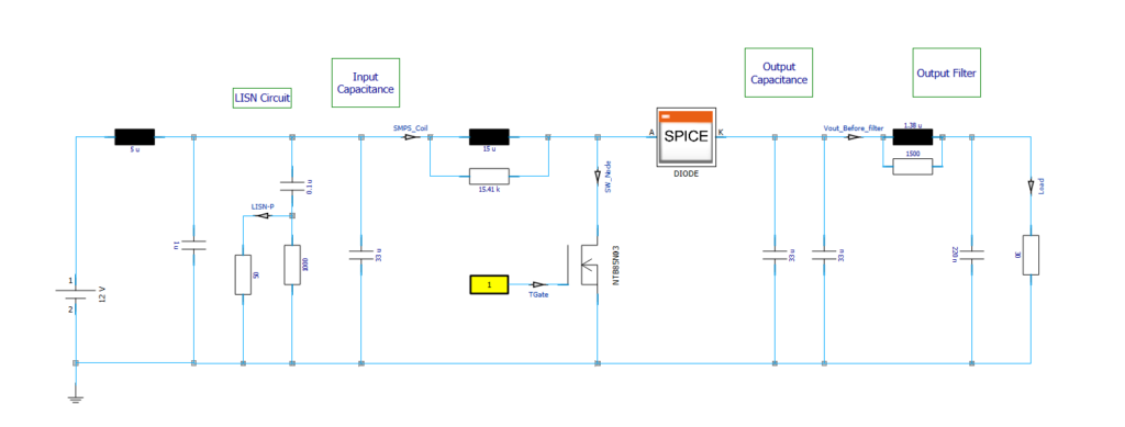
Note that the yellow block is the port controlling the switching of the transistor. The diode model is imported as a SPICE block. The control signal is switching the n-MOSFET transistors with the periodic rectangular pulses. The switching frequency is fixed at 1.25MHz with a 36% duty cycle in order to achieve 17.5V DC output voltage with 580mA. We can see that the +12V DC line is connected with the coil and drain pin of the n-MOSFET transistor. During the transistor’s switching “ON” period, the main power line connected to the drain pin of n-MOSFET is periodically pulled down to GND. Thus, this node is called as switching node and will have a strong influence on the EMC at high frequency.
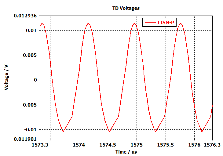
To simulate the DCDC converter, the circuit transient simulator is used here. The transient switching behavior of the transistor is simulated and the simulation is typically stopped after the load voltage reached the required DC voltage level. The switching noise spectrum at the battery input is recorded using a so-called Line Impedance Stabilization Network (LISN). For this particular example, where ideal circuit elements were simulated, the noise at the LISN has a mainly sinusoidal waveform. This is shown in Figure 2.
Although very similar to a sine wave, the wave does have harmonic components. The LISN spectrum shows a continuous decay of higher harmonic frequencies. The Figure 3 below shows the spectrum at the LISN from this converter:
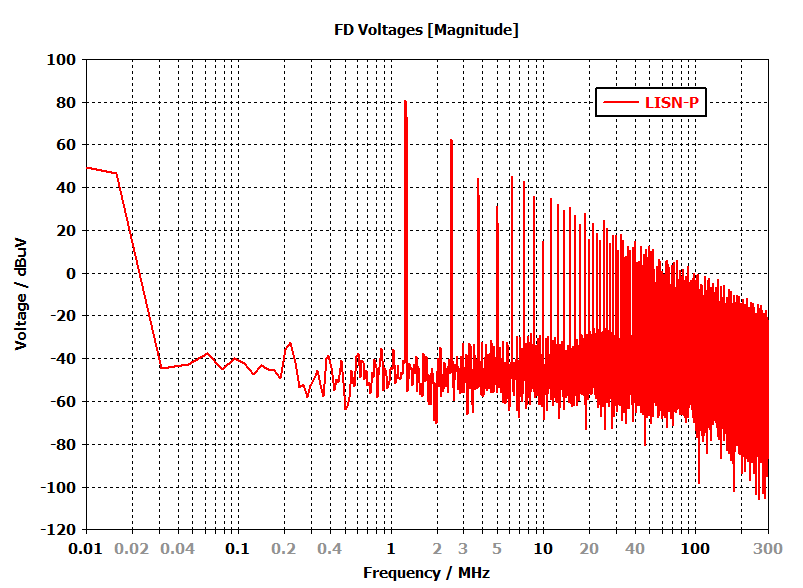
In Figure 3, we can clearly see the peaks at the switching frequency and the higher harmonics. Since the switching frequency is fixed at 1.25 MHz, we can see a sharp peak at this frequency. In order to reduce this amplitude at LISN, the spread spectrum technique to the controlled signal switching at the transistor will be applied.
Spread Spectrum Clock Generation (SSCG)
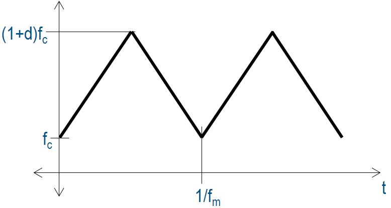
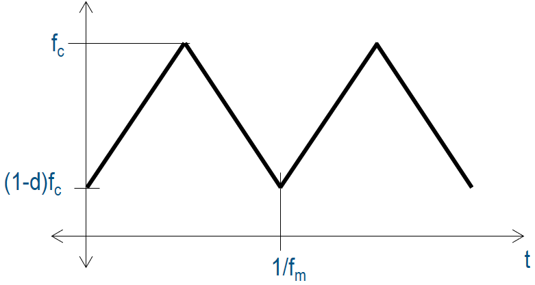
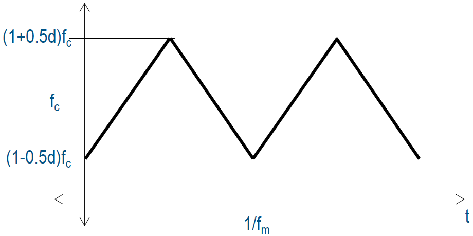
The basic idea of SSCG (spread-spectrum clock generation) is to apply a modulation to the switching signal instead of using a fixed switching frequency. The switching frequency of the transistor is modulated with a modulation signal that has a fixed modulation frequency (fm) and an amplitude. Commonly, the signal is modulated using a triangle function. The amplitude of this triangle signal determines how much the switching frequency is varied from its nominal frequency (fc). This is called the spreading rate (d) and it is typically given in percentages.
If the switching frequencies are varied to a higher frequency than the nominal frequency, the term “up spreading” is used. Similarly, if the variation is towards frequencies lower than the nominal frequency, the process is called “down spreading”. Finally, when the switching frequencies are varied to both directions symmetrically, the term “center-spreading” is used. For a better understanding, please refer to Figure 4, Figure 5, and Figure 6.
DCDC Converter Simulation with Consideration of the Spread-Spectrum
When simulating the DCDC converter with CST Studio Suite®, we can also consider the spread-spectrum modulation of the switching signals controlling the transistor. This helps the designer to get more realistic results which are closer to measurement results if the spread-spectrum technique is also applied to the physical product.
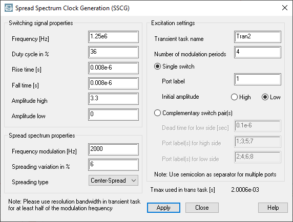
In order to consider the spread spectrum, CST Studio Suite includes a macro to define the switching signal properties as well as the SSCG properties. The SSCG macro can be found in the CST Studio Suite® 2023 schematic editor under Post-Processing–> EMC Workflow–> Spread Spectrum Clock Generation. The spread-spectrum properties can be typically obtained from the datasheet of the simulated converter. For DCDC converters the spreading rate is typically in the range of 6% up to 10%. Figure 7 illustrates the user interface of this macro.
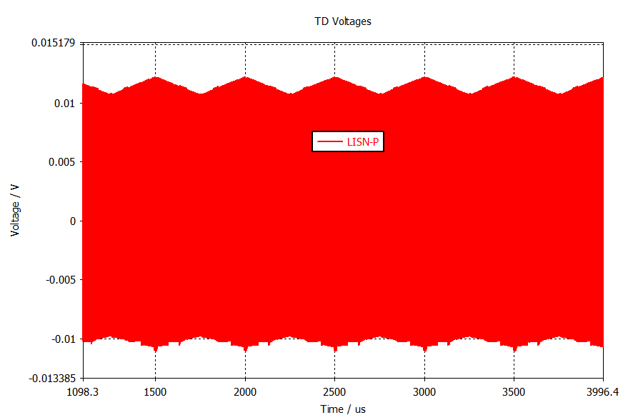
The macro creates a transient simulation task and assigns the spread-spectrum signal to the port controlling the switching of the transistor (s. Figure 1). After executing this transient simulation task, several time signal results are available. In this example, the time signal result of the LISN is shown in Figure 8. As the switching frequency is modulated with a triangle signal, the noise coupled to the power line also exhibits an envelope corresponding to the modulation shape.
Fourier Transform and Window Function
The spectrum of a periodic signal is calculated using a Fourier transform. The periodic signal can be represented by a Fourier series and the spectrum of this periodic signal is given by Dirac pulses at distinct frequency points. In a real world applications, we often deal with finite length signals. To assume the periodicity of this signal, time gating or windowing is applied before performing the Fourier transform.
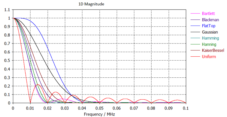
The simplest form of time gating or windowing is a uniform or box car window function. However, this window function produces a high side-lobe level in the spectrum. The appearance of these side-lobes is also called spectral leakage. In order to reduce the high side-lobe level, a non-rectangular window function can be applied. Several window functions are available in CST Studio Suite®, and Figure 9 shows the associated spectra of all supported window functions.
Resolution Bandwidth (RBW)
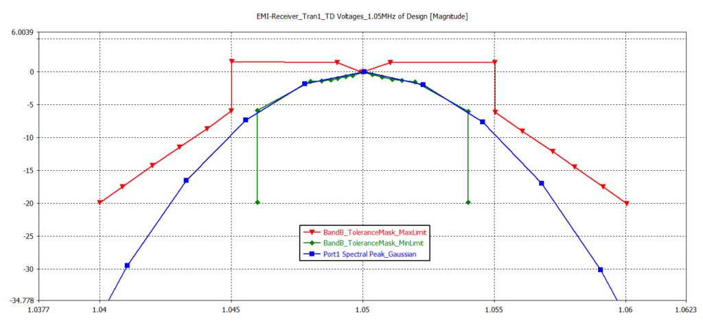
In general, the spectrum of uniform window function has the narrowest main lobe, but high side-lobes, whereas the Gaussian window and flat top function have wider main lobes, but very low side-lobes (Figure 9). The standard CISPR-16 specifies the mask tolerance for the window function spectrum. Any window function can be used, as long as it is located within the tolerance mask. In most EMC applications, the Gaussian window function is used since the spectrum of it located inside the tolerance mask.
The width of the window function determines the frequency resolution. It is known as the resolution bandwidth (RBW). Obviously, a wider window width results in a smaller RBW. Thus, a higher frequency resolution can be achieved. The CISPR-16 standard also specifies the RBW to be applied during the measurement for different frequency bands.
| Fstart | Fstop | RBW | CISPR-Band |
| 9 kHz | 150 kHz | 200 Hz | A |
| 150 kHz | 30 MHz | 9 kHz | B |
| 30 MHz | 1 GHz | 120 kHz | C/D |
| 1 GHz | 18 GHz | 1 MHz | E |
Finally, after the time signal is being windowed, the Fourier transform will be applied in order to obtain the final spectrum.
EMI Receiver Template-Based Post-processing
If the spread-spectrum is used in a simulation, the spectrum of this signal should not be calculated using a one-time calculation of the Fourier transform, but instead multiple Fourier transforms should be performed over time windows. This is mainly due to the variation of the switching frequency over the time (see Figure 8) which needs to be taken into account for the final spectrum. Therefore, the EMI receiver template-based post-processing is used to calculate spectrum of the spread-spectrum signal.
The EMI receiver template implementation is based on the EMI receiver measurement using the Fast Fourier Transform (FFT) method. This receiver has pre-defined RBW and window function settings which complies with the CISPR-16 specification. The FFT based receiver performs shifting of the window function over the signal. The shifting between each window function has about 90% overlap in order to capture the uncertainty in the signal. The Fourier transform for each of these shifted windows is performed subsequently. This will results in several spectra results.
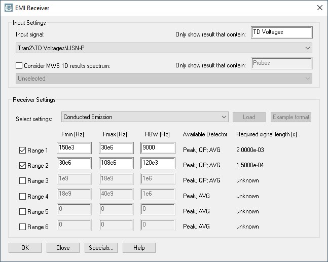
At the final stage, these spectra are input into the detectors to obtain the final spectrum. Similar to the measurement, the EMI receiver template supports three detectors, “Peak”, “Quasi-Peak” and “AVG”. However, the EMI receiver template uses “Peak” and “AVG” detectors by default. The “Quasi-Peak” detector can be activated manually and it requires a longer calculation time. The “Peak” results are obtained by detecting the peak value at each frequency point, whereas for the “AVG” result, averaging is performed at each frequency point. The Figure 11 shows the dialog window of the EMI receiver template. Similar to SSCG macro, the EMI receiver template can be accessed in design studio through Post-Processing–> EMC Workflow–> EMI Receiver.
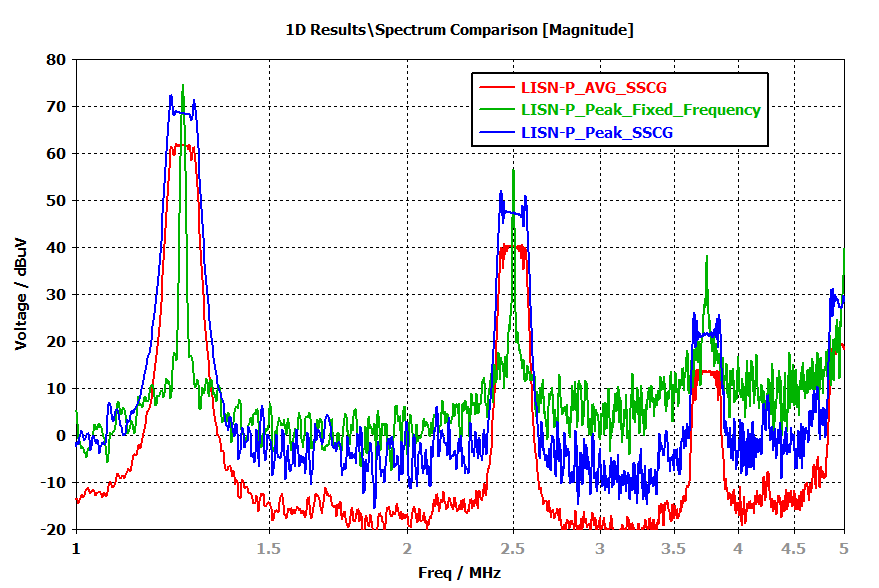
The spectrum comparison between a fixed switching frequency and SSCG can be seen in the following Figure 12. Because the spread-spectrum technique varies the switching frequency, the spectrum received using the SSCG is wider than the spectrum using a fixed switching frequency. The width corresponds to the spreading rate. The spread-spectrum technique produces also lower amplitudes than the amplitudes of the fixed switching frequency. A considerable reduction of the amplitude can be seen using an AVG detector. In this example, it is approximately 13 dB lower compared to the spectrum using a fixed switching frequency.
Summary
The spread-spectrum clock generation can be considered in EMC simulations CST Studio Suite®. This technique allows to reduce the magnitude of the noise spectrum without any modification of the layout or components. It is also important to note that the SSCG produces varying time signal results and therefore the EMI receiver template shall be applied in order to get a more realistic final spectrum. Consideration of both these features in the CST Studio Suite simulation helps the designer to get more realistic results closer to measurements system.

Join a community of simulation enthusiasts focused on advancing the use of SIMULIA simulation solutions in science and engineering! It’s free and easy. Start a discussion with other members of the SIMULIA Community. Talk through your simulation questions with peers, SIMULIA experts, and SIMULIA Champions. Apply to be an author to create posts, share useful tips you discovered for SIMULIA software, and establish yourself as a thought-leader. The SIMULIA Community is home to both SIMULIA product users and SIMULIA subject matter experts around the world.

Richard Sjiariel joined Dassault Systemes Deutschland since June 2021. His current position is SIMULIA Industry Process Consultant with the main focus of EMC simulation. From 2015 to May 2021, he was a hardware developer at Continental Automotive GmbH, Germany, where he was responsible for automotive display development, such as power supply concept, FR4-PCB and Flex-PCB layout architect, signal- and power integrity simulation and measurement, as well as EMC measurement according to CISPR-25. Before joining Continental, he was working 8 years as application engineer at CST. He gave technical support, training and webinar with the application area signal integrity and power integrity. He finished his M.Sc. degrees in electrical engineering from University of Wuppertal in 2006.