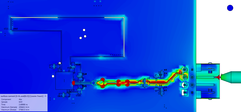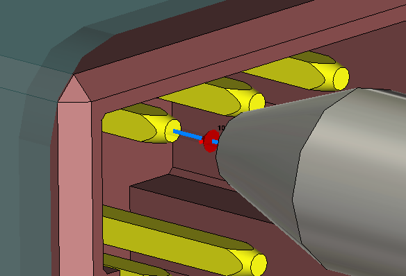
ESD contact discharge is usually tested in the lab by physically connecting a high-voltage probe to a prototype of the device under test (DUT) at a specific location, such as a connector pin. Additionally, a non-contact test is carried out by placing the probe at varying distances from likely discharge points on the DUT.
These tests must be repeated for every possible connection & discharge path, making ESD testing time-consuming and expensive. It can also be difficult to understand the root causes of failure from the limited output of an ESD test. Many prototypes can be damaged or destroyed in the testing process.
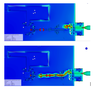
Virtual testing with simulation can accelerate ESD analysis, reducing development time and cost. Both the test equipment and the DUT are created and connected in the virtual environment, with waveforms generated to replicate the real-world tests. 3D visualization of simulation results shows the exact path of currents through the device, helping engineers understand the causes of ESD problems and develop design mitigation strategies.
Challenges of ESD Analysis and Mitigation
ESD is a significant risk for electronic devices: Sensitive low-voltage electronic components such as integrated circuits (ICs) can easily be damaged by high-voltage pulses. Even if catastrophic damage does not occur, permanent damage may occur, reducing the life of the device or cause unexpected behavior.
ESD occurs when a static electric charge is generated on an object and then discharges to earth via an electronic device. This often happens if a human user picks up an electric charge from friction with their clothing, the floor or furniture, and can also come from moving machinery such as vehicles or conveyor belts or from electrostatic induction from other charged objects.
For ESD to occur, there must be a path between the charged object and the ground through the device. This path can be either direct contact or close proximity contact in which case an arc through the air gap will form. In dry air, static charges can build up more readily, with faster rise times, and higher peak amplitudes, while in humid air, non-contact discharge can form with longer arcs, more slowly rising with lower peak amplitude.
The large number of variables in conditions, contact type and arc type mean that analyzing ESD risk requires a long series of physical tests on a significant number of expensive prototypes. Tests have to occur late in the product cycle when detailed prototypes are available. If issues during ESD testing are found, there are a number of steps required that may cause delays and impact the scheduled release date. Steps include understanding the causes of any failure and redesign and rework of the device to mitigate the issue for the next prototype.
ESD testing on modern devices can be particularly complicated as additional components are now integrated into a single device, such as a system on chip (SiP). The ESD protection for each individual IC must be harmonized with the system-level ESD protection (SEED). Ensuring safe voltages and currents at all ICs can require trade-offs in terms of component placement, informed by a large number of tests.
Benefits of Electrostatic Discharge Simulation
Simulation offers a faster alternative to testing. Unified modeling and simulation (MODSIM) makes it easy to turn CAD geometry data into a simulation-ready virtual prototype of the DUT and the test equipment set-up. An excitation at the tip of the virtual generator creates an ESD pulse, and the simulation calculates its propagation through the device. 3D field monitors can visualize the exact path of currents flowing through the device, and virtual field probes can be placed anywhere in the virtual space, including inside the device.

Evaluating ESD susceptibility virtually means that problems can be identified and resolved even before construction of the first prototype. This approach enables engineers to get the design right first time, saving on prototyping costs and reducing the risk of project delays caused by issues discovered during testing.
The SIMULIA ESD Simulation Solution
CST Studio Suite contains state-of-the-art electromagnetic solvers for simulating complex components and systems accurately and efficiently. ESD is inherently a transient phenomenon, and it can be simulated effectively using the 3D Time Domain Solver. The Time Domain Solver also offers highly efficient 3D meshing that is robust enough to deal with poor CAD geometry. Complex geometries are represented accurately and virtual tests can be run rapidly. Design of Experiments (DoE) capabilities allow automated testing of various scenarios with clear visualization and comparison of large datasets.
The ESD susceptibility analysis workflow starts with building the DUT’s virtual twin. 3D geometry and PCB or IC layouts from standard CAD and EDA tools can be imported into the virtual environment and converted into simulation-ready models with automatic clean-up and meshing.
Pre-defined ESD-specific templates, such as 3D models of ESD generators and ESD pulse excitations, available from the CST component library, help users define their simulation set-up. The ESD generator models have been developed and validated to comply with international standards such as ISO 10605 and can accurately model real-world ESD test set-ups. Users can build representations of standard tests that replicate the set-up found in the lab.
Both contact and air-gap ESD generators can be simulated. In the case of an air gap (in other words, where voltage breakdown in the air causes an arc, an electromagnetic simulation is first performed to calculate possible arc paths at different voltages using Paschen’s law, and to generate a SPICE model that represents the non-linear electromagnetic properties of the arc. This then forms the basis for the time domain simulation of the ESD pulse, with true transient co-simulation combining the SPICE circuit model with the 3D simulation model.

The simulation produces several ESD KPIs and a 3D visualization of electromagnetic fields and surface currents around the device. Using virtual probes, users can view voltages at any point in the structure throughout the duration of the pulse. Users can generate all the KPIs that a physical test would provide, and some that would be impossible to measure.
Conclusion
Electrostatic discharge (ESD) can cause errors and device failures and affect the safety and reliability of a device market. Successfully bringing an electronic product to market means meeting legal ESD regulations and ensuring that a device is protected from ESD exposure.
Electromagnetic simulation can be used to analyze ESD risk on a device without the cost of building and potentially destroying physical prototypes. A virtual twin contains all relevant data about the product and can be used to accurately represent product behavior in a virtual test using simulation. Engineers can quickly build a virtual twin of their product from the design data thanks to the unified modeling and simulation (MODSIM) approach enabled by Dassault Systèmes tools on the 3DEXPERIENCE platform.
With virtual testing, engineers can understand ESD risk from the earliest stages of design and can develop protection and mitigation strategies for individual components or the entire device. Virtual testing helps prevent problems being discovered late in development when rework is expensive and risks delaying the entire project. It also reduces the risk of device failures after launch and the cost of recalls.

Interested in the latest in simulation? Looking for advice and best practices? Want to discuss simulation with fellow users and Dassault Systèmes experts? The SIMULIA Community is the place to find the latest resources for SIMULIA software and to collaborate with other users. The key that unlocks the door of innovative thinking and knowledge building, the SIMULIA Community provides you with the tools you need to expand your knowledge, whenever and wherever.

