
*The following was co-authored with Reiner Welzer, an Application Engineer at Inova Semiconductors GmbH. He has over 20 years of experience in signal and power integrity and EMC compliant designs of RF and analog signal PCBs. In recent years, he has worked extensively on ESD protection of electronic circuits, especially for automotive.
Coupled Microstripline Modeling
With the data transmission over a single twisted-pair cable, the connection on the PCB is realized using an edge-coupled surface microstrip conductor. Mostly differential signaling is used for high-speed data transmission. This provides a good electromagnetic compatibility (EMC). Typically, an edge-coupled surface microstrip conductor with a nominal line impedance of 100 Ω is used and located at the TOP layer. Figure 1 shows the dimension of edge-coupled microstrip line used for the simulation, which delivers 100ohm differential line impedance.
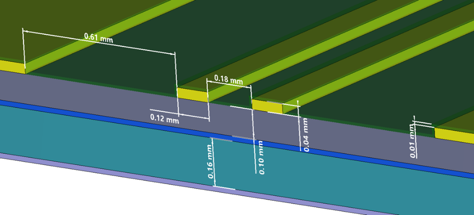
For a line impedance calculation, the correct material property and the modeling of the correct solder mask shape are important. As shown in Figure 1, the modeling of the solder mask is realized as a thin skin, covering the microstrip conductor.
As the differential line is connected to the cable through a plug, a possible ESD event is very likely to occur at this plug. Such an ESD event generates very high voltage and current peaks within a short time range ( < 1 ns) and it can cause damage to the electronic components. In order to avoid this, ESD protection components should be connected to both conductors of the differential line. Very often TVS (Transient Voltage Suppressor) diodes are used for such applications. They have a very fast response-time and limit the voltage to a certain value within a short time.
With a high-speed data rate of 6 Gbps, it is important to use small component package sizes with low parasitic elements. For the analyzed geometry, we were using the ESD protection diode PESD5V0C1BLS-Q from NEXPERIA [1]. This device has a maximum diode capacitance of 0.3 pF and a small package size of 1 mm x 0.6 mm x 0.47 mm. In the simulation, the ESD diodes are defined using “lumped elements”. They are reproduced by their parasitic capacity only. “Lumped elements” are CST internal elements, which can represent R, L, C components. Figure 2 shows the simulation model of the differential line including the ESD diodes.
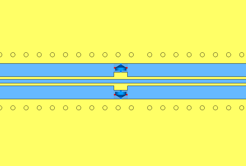
In Figure 2 it can be seen that the landing pads of the ESD components on the differential signal line are wider than the trace. Obviously, the cross-section change at this particular position leads to a line impedance change. Depending on the size of the impedance change, there is an impact to the signal integrity.
Pre-Layout TDR Simulation
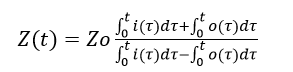
A well-known method to analyze the line impedance along a transmission line is the time domain reflectometry method (TDR). It works similarly to the radar principle, where a pulse is transmitted and the reflected signal is recorded back at the input side. Information about the impedance curve can be obtained by evaluating the reflected signals. CST Studio Suite can also perform TDR simulation using either the time domain- or frequency domain solver. For this pre-layout investigation, we use the frequency domain solver. This is justified because of the relatively simple structure for discretization and its small size compared to the wavelength. As the frequency domain solver delivers only the S-Parameter results, we calculate the TDR results by post-processing the return loss S-Parameter S11. With a Gaussian signal defined as the input signal, the output signal can be reconstructed from the return loss information. We calculate TDR by applying Equation 1.
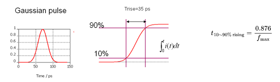
The maximum frequency range defined in the simulation is 8.4 GHz, which corresponds to the 10%-90% rise time of 104 ps.
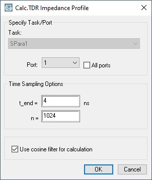
CST Studio Suite can perform this calculation automatically using the template-based post-processing “TDR calculation from S-Parameter”, as shown in Figure 4.
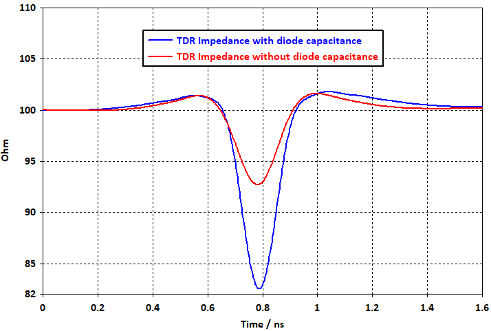
Although the diode capacitance value is considerably small (0.3 pF), it has to be considered when performing the TDR simulation. It reduces the nominal line impedance (100 Ω). Figure 5 illustrates the comparison with – and without considering this capacitance.
Layout Modification
A maximum allowed impedance variation of ± 10% is typically set when designing high-speed data lanes. With a 100 Ω reference impedance, we can see from Figure 5 that the curve drops down to
83 Ω. This would fail the lower limit (90 Ω) of the requirements. To fulfill the impedance requirement, a layout optimization around the ESD diode location must be performed.
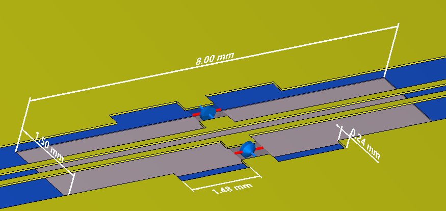
Since the ESD diode capacitance reduces the line impedance in this region, it is necessary to compensate this effect by reducing the capacitance per meter of the transmission line. The most effective method to do this is to cut out the reference plane below the ESD diodes. The optimal size of the recessed ground area can be found by simulation. Figure 6 shows an optimized configuration of the modified reference plane for a certain layer construction after several simulation iterations.
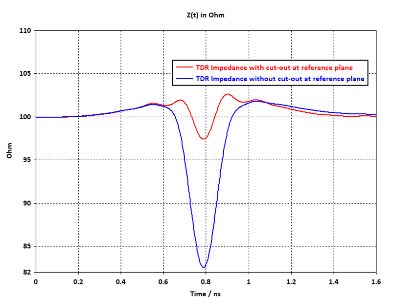
The corresponding impedance curve improvement can be seen in Figure 7.
Please note that the cut-out in the ground plane may allow crosstalk from and to other switching or interference signals. Therefore, it is recommended not to route any sensitive signal line below this cut-out. In the PCB layout design tool, this can be ensured by creating a restricted/keep-out area.
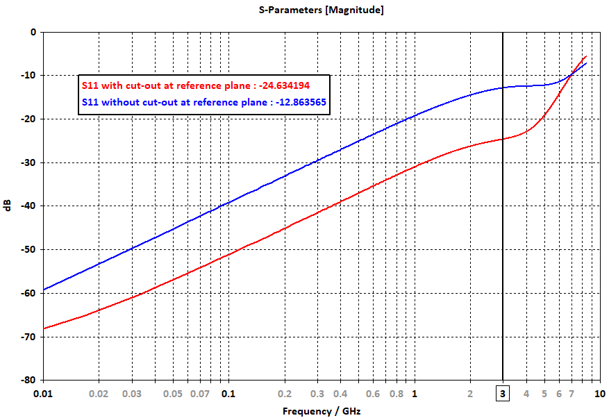
The improvement of the line impedance can also be seen from the return loss S-parameter S11
(Figure 8). An improvement of around 12 dB for the return loss can be observed. This also means an improvement for the signal integrity.
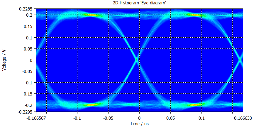
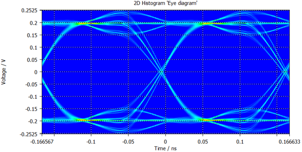
The better signal integrity behavior of the recessed reference plane can also be demonstrated by comparing the eye-diagram results. The used digital Pseudo Random Bit Sequences (PRBS) have the following properties:
- PRBS12
- Differential voltage level ± 200 mV
- Rise and fall time of 80 ps and period length corresponds to 3 GHz
Figure 9 and Figure 10 show the eye diagram for both layouts.
Measurement Comparison
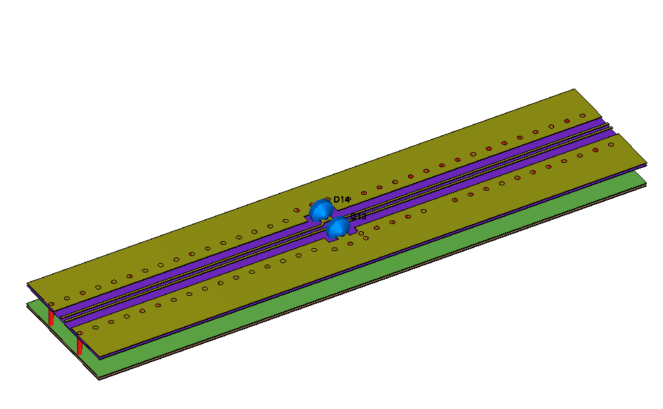
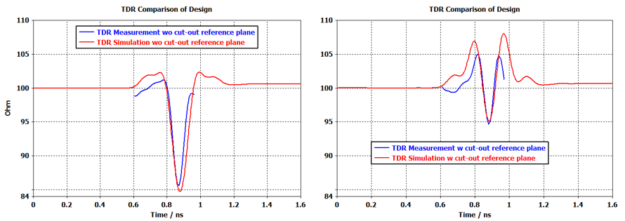
To confirm the simulation results, a PCB layout with optimized parameters (found by CST Studio Suite simulation) has been created. The TDR impedance measurement has been performed with a differential TDR measurement-system from Sequid. During the measurement, the transmission line was connected via SMA sockets. For the simulation, it is not necessary to consider the connectors because they only increase the computing power and time and have no influence to the line impedance around the ESD diodes. The end of the differential line can be left open.
The manufactured PCB prototype for the measurement is a standard FR-4 board with 4-layers and a total thickness of around 1.6 mm. The differential pair dimension differs slightly from the one used in the pre-layout investigation, but the reference plane cut-out dimensions remain the same. Figure 11 shows a section of the PCB layout prototype used for measurement comparison by CST Studio Suite.
The comparison of the line impedance results between measurement and simulation is shown in Figure 12. The good agreement to the measurement confirms the simulation with CST MWS.
Conclusion
To transmit high-speed data signals, it is important to achieve a smooth line impedance curve for the whole high-speed data lane. The signal integrity requirements are typically ± 10% from the reference impedance. In this blog article, we presented the 3D layout simulation and optimization of such a transmission line using CST Studio Suite. We demonstrated the benefits of using this simulation tool in the pre-layout phase, especially regarding the development time. We showed that it is important to respect the ESD diode component (capacitive information) during the optimization, to achieve more realistic results. Finally, a good agreement between simulation and measurement confirmed the accuracy of the simulation results with CST Studio Suite.
References
[1] https://www.nexperia.com/products/esd-protection-tvs-filtering-and-signal-conditioning/automotive-esd-protection-and-tvs/automotive-esd-protection/PESD5V0C1BLS-Q.html
[2] CST Studio Suite 2024 Online Help.

Interested in the latest in simulation? Looking for advice and best practices? Want to discuss simulation with fellow users and Dassault Systèmes experts? The SIMULIA Community is the place to find the latest resources for SIMULIA software and to collaborate with other users. The key that unlocks the door of innovative thinking and knowledge building, the SIMULIA Community provides you with the tools you need to expand your knowledge, whenever and wherever.

Richard Sjiariel joined Dassault Systemes Deutschland since June 2021. His current position is SIMULIA Industry Process Consultant with the main focus of EMC simulation. From 2015 to May 2021, he was a hardware developer at Continental Automotive GmbH, Germany, where he was responsible for automotive display development, such as power supply concept, FR4-PCB and Flex-PCB layout architect, signal- and power integrity simulation and measurement, as well as EMC measurement according to CISPR-25. Before joining Continental, he was working 8 years as application engineer at CST. He gave technical support, training and webinar with the application area signal integrity and power integrity. He finished his M.Sc. degrees in electrical engineering from University of Wuppertal in 2006.