The following post was originally published in March 2021.
The SIMULIA Blog is committed to providing high-quality simulation content that is technical and digestible for a broad audience of simulation enthusiasts. And that means connecting SIMULIA experts to our users by giving them a platform to educate and inform. Our newest series will focus on very technical concepts and simulations, delving deep into a particular topic. Today we are excited to have Dr. Andreas Barchanski, SIMULIA Electromagnetics Industry Process Consultant Senior Manager, discuss the concept of loop and partial inductance and how to extract RLC models from electromagnetic simulation. He will also explain how the new pRLC solver in CST Studio Suite improves the simulation of partial RLC models, and will use a package model with bond wires to demonstrate the most important result findings.
And don’t forget to visit the SIMULIA Community for the simulation models Dr. Barchanski used in this post.
In today’s blog entry I will discuss the concept of loop and partial inductance and how to extract RLC models from electromagnetic simulation. I will explain how the new pRLC solver in CST Studio Suite improves the simulation of partial RLC models. Finally, I use a package model with bond wires to demonstrate the most important result findings.
The idea to extract equivalent models from field simulations is probably as old as electromagnetic field simulation itself. Condensing the properties of a physical structure into a lightweight model that describes its behavior adequately allows the usage of such models for further processing, for example in system or circuit (SPICE) simulations. Typical examples in the world of electronics are: a bus bar connecting high power components, a signal trace on a PCB, a long via in a high speed channel or a bond wire in a package. Obviously, a very natural description for every electrical engineer is the usage of lumped element networks constructed from resistance, inductance and capacitance (RLC). This approach works well as long as the structure size is smaller than one tenth of the smallest wavelength of interest.
In electromagnetic compatibility (EMC) and electronic design automation (EDA) applications, the inductance of the structure is of particular interest as at frequencies above the kHz range it becomes the governing factor to the overall impedance. Most electrical engineers will also immediately think about signal ringing when they hear the term inductance. Thus, today’s post will start with a more in-depth look at the calculation of inductance from electromagnetic field simulation.
Traditionally, the inductance is defined as the magnetic flux through a surface S enclosed by a line current 𝐼. Because the magnetic flux can be calculated from B by integrating over the surface, we obtain:
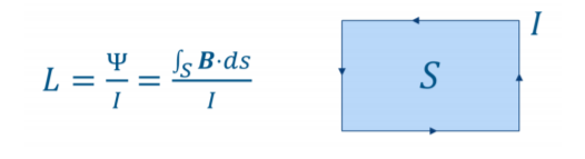 This is the so-called loop inductance, as it always requires a closed loop to define a surface. It is very straightforward to estimate the closed loop inductance from a full-wave solver. Define a conductive loop closed by an S-parameter port. Convert the S-parameter to Z-Parameter or directly to the inductance using template-based post-processing in CST Studio Suite. With the same steps, the resistance of the loop can also be calculated. The loop inductance is closely related to the physical behavior of the system as a current always flows in a loop. However, it is not necessarily the most relevant result for an electronics designer.
In modern electronics systems, the full current loop can be geometrically quite complex flowing over multiple PCBs, cables and connectors. A designer is often interested how a particular section of the current loop contributes to the overall inductance. This is the starting point for the concept of partial inductance. If we want to calculate the contribution from just a section of the current – for example just the bottom section of the rectangle in the figure above – we cannot employ the above formula as there is no longer a closed loop. Instead of calculating field quantities like B we need to take a detour and calculate a suitably chosen vector potential A which is related to the magnetic field as 𝑩 = 𝛻 × 𝑨. I will not go into the details of calculation as it involves some heavy field theory but the main point is that this calculation cannot be performed by a “standard” full-wave solver and we need a specialized solver to do so.
Traditionally, the partial inductance calculation leads to a numerical method called PEEC (Partial Element Equivalent Circuit method). The method is closely related to the method of moments (MOM) and has been employed for many years for the calculation of partial quantities. However, this approach has certain drawbacks: it requires a special mesh that is difficult to apply to complex CAD structures. It also has some issues with magnetic material properties and scales badly with the number of mesh elements.
Therefore, we at SIMULIA have decided to re-think the partial extraction from ground up using a different approach that does not suffer from the above-mentioned difficulties. The pRLC solver in CST Studio Suite is based on a Finite Element Method (FEM), which has proven over the past years to be an efficient choice for many applications. Our solver can deal with arbitrary geometries and can even use curved mesh elements. It scales very efficiently, allowing us to use it straight away even on complex imported CAD geometries. It can handle high permittivity and high permeability materials and is able to solve from DC to full-wave without approximations. The extracted RLC values are plotted in the CST Studio Suite result tree for direct reading or they can be exported as SPICE files. Both single-frequency and broadband export is possible.
The main application area of the partial RLC extraction are typically structures much smaller than wavelength: This can be bus bars in power electronics applications where the frequency of interest is in the MHz range or bond wires in a package where the frequency can be even several GHz but the length of such bond wires is rather short. Extracting human readable values of RLC is a very important advantage of the pRLC approach and helps in understanding the behavior of the structure. This works best for models where the number of components is small as reading and interpreting a system with a high number of elements becomes increasingly difficult. For system level simulations where a black-box type of model is required, I typically recommend using a full-wave solver and S parameters. If needed, S parameters can be translated into a SPICE model using vector fitting.
In the example below, we will take a look at the extraction of the inductance of a package bond wire with a fan out trace. The package has been designed using state of the art package design software. The design was imported directly into CST Studio Suite using the powerful built-in import interface that additionally allows users to choose the nets and sections of the package to be imported. For a clearer understanding, I have colored the model: The net of interest B_DQ_14 is colored blue, VCC is red and GND is green. The substrates are included in the simulation but have been hidden in the figure below.
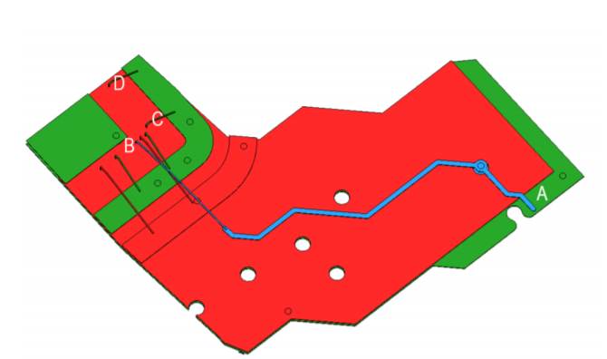
For the partial inductance, it is quite straightforward to define a route from point A to point B as being the inductance of the package connection. However, for the loop inductance, there are multiple possibilities for the current loop to close that depend on the actual routing inside the chip. If we want to separate the properties of the package from the actual chip this is only possible by a partial extraction. Still, it is worth to take a look at the results and compare the partial inductance, the loop inductance calculated using the partial approach, and the loop inductance calculated using a full-wave solver. For demonstration purposes, I have chosen bond wire C and D. In order to close the loop I add metallic connections from B to C and B to D respectively.
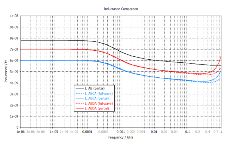
The simulations take around 7 minutes for the partial RLC solver and 15 minutes for the fullwave solver on a laptop equipped with an Intel i7-7820HQ processor. The inductance for the different cases is plotted in the above figure. We can observe the typical behavior: Below 100 kHz, the inductance value is highest, this region is often called DC inductance. Around 1 MHz it decreases due to the skin effect and around 100 MHz we have the so-called AC inductance. In many cases, these two regions are much more flat than in our example. In our example, the transition range from DC to AC is very broad because of the small dimensions of the conductor in our package model. Around 1 GHz we can observe an increase of the values. This is the frequency where the electrical length of the loop compared to wavelength is about 𝜆/10 and we no longer can use a single inductance value to describe the electrical properties of the loop accurately. The partial inductance AB is higher than the loop inductances ABCA & ABDA. This is a general finding, because when the full loop is included the return current decreases the resulting inductance.
For the calculation of the resistance, exactly the same approach as for the inductance can be used. For the capacitance, however, we need to solve another step, which is quite similar to an electrostatic simulation. The concept of partial capacitance can be confusing as the physical interpretation is lacking. Capacitance is a property of conductive bodies, so two conductive bodies will be described by one capacitance value (omitting self capacitance). However if there are multiple nodes defined on one conductor, as it is needed for the partial inductance calculation, then the capacitance of the conductive body needs to be spread among these nodes in order to generate a consistent model for example for SPICE export. This is the idea behind the concept of partial capacitance.
In this blog post, I have tried to explain some main ideas behind the extraction of RLC values through electromagnetic simulation. Key points to remember are:
- Single RLC values can be used to describe the properties of electrically small structures.
- The loop-inductance is what physically matters, but extracting the partial inductance can be very helpful for electronics designers as it allows estimation of the contribution of separated sections of the structure.
- The frequency dependent inductance exhibits two regions typically called DC and AC inductance.
- The concept of partial capacitance is employed to distribute the capacitance among multiple nodes on one conductive body.
I hope you have enjoyed reading this post as much as I did writing. Let me know your comments below or engage in a discussion in the SIMULIA Community. You can find the simulation models in the SIMULIA Community.
We hope you enjoyed this post and have learned about the main ideas behind the extraction of RLC values through electromagnetic simulation. If you would like to learn more about this topic, or about anything regarding electromagnetic simulation, visit the SIMULIA Community. Dr. Barchanski encourages everyone to visit the community to ask questions and to engage in any additional discussion with him. We look forward to seeing you there!
SIMULIA offers an advanced simulation product portfolio, including Abaqus, Isight, fe-safe, Tosca, Simpoe-Mold, SIMPACK, CST Studio Suite, XFlow, PowerFLOW and more. The SIMULIA Community is the place to find the latest resources for SIMULIA software and to collaborate with other users. The key that unlocks the door of innovative thinking and knowledge building, the SIMULIA Community provides you with the tools you need to expand your knowledge, whenever and wherever.

Andreas is a senior solution consultant for electromagnetic simulation at Dassault Systèmes in Darmstadt, Germany. After receiving his PhD in numerical electromagnetics from the Darmstadt University of Technology in 2007 he joined CST which later became a part of Dassault Systèmes. His main interest lies in the simulation of electromagnetic compatibility of electronic systems, ranging from high-speed to power electronics.