In this blog post, we show how to combine different tools and techniques within the SIMULIA CST Studio Suite® environment to design microwave filters. We apply these workflows to the design of filters based on Substrate Integrated Waveguide (SIW) and Empty Substrate Integrated Waveguide (ESIW) technology.
SIW and ESIW technologies
Most modern wireless systems require electromagnetic (EM) filters: cellular base stations, satellite telecommunications, radar systems, etc. The function of such a device is to filter a signal’s spectrum, generally while also maintaining the integrity and avoiding thermal noise and unwanted interference.
Over the past two decades, substrate integrated waveguide (SIW) technology [1] has been used to develop filters at high frequencies. This technology is a good trade-off between the benefits of waveguides, having low losses and high power handling capability, and planar circuits, offering tight integration and low cost.
More recently, some authors have proposed a technology based on waveguide technology that is compatible with integrated planar circuits, the so-called empty substrate integrated waveguide (ESIW) [2]. This approach enables the direct access of the waveguide to the microstrip line. Thus, a circuit with low losses, fully integrated in a planar substrate, can be developed.
On the other hand, filter design is often a cumbersome task, especially if the filter specifications are challenging. In this blog post, we show how to combine different tools and techniques to design filters based on SIW and ESIW technology efficiently. In particular, we present two specific workflows, which filter designers can also apply to their own developments regardless the specific technology.
Before describing the workflows to design microwave filters within the CST Studio Suite® environment, we introduce the specific tools and solvers that we will need during the design process.
SIMULIA filter simulation technology
CST Studio Suite® is a high-performance 3D electromagnetic (EM) analysis software package for analyzing/designing EM components and systems. It incorporates several electromagnetic field solvers suitable for different applications. In particular, for filter design, CST Studio Suite® incorporates two suitable 3D solvers:
- The Frequency domain solver, which is a powerful multi-purpose 3D full-wave solver, based on the finite element method (FEM). It includes a model-order reduction (MOR) feature, which speeds up the simulation of resonant devices, as well as a moving mesh technique, which is important for reducing mesh noise in highly sensitive filter simulations that enables optimization convergence.
- The Eigenmode solver, which is a specific solver for simulating resonant components. Common applications of the eigenmode solver include coupled-resonator filters, high-Q particle accelerator cavities, and slow wave structures such as travelling wave tubes. It also supports open boundary problems which is very important for models based on SIW or other planar technologies.
Filter Designer 3D (FD3D) is a coupling matrix synthesis and analysis tool for the design of bandpass filters and diplexers. It also offers automation for 3D model creation and optimization of distributed filters implemented in various technologies such as coaxial cavity, waveguide, planar, etc.
Fest3D is a software tool capable of analyzing complex passive microwave components based on waveguide and coaxial cavity technology very efficiently. This is achieved by a divide-and-conquer approach in which the different parts of the component are solved with the most efficient method and connected to the other elements through the EM modal expansion on the interfaces (ports). On top of that, Fest3D offers advanced automatic design tools for bandpass, dual-mode and lowpass filters based on waveguide technology.
SIW filter design workflow
A general yet automated workflow within the CST Studio Suite® environment is outlined in the following steps:
- Define the filter specifications in FD3D and select from a range of topologies that would provide the appropriate coupling matrix for the synthesis.
- Select the desired 3D models in the component library that represent the different parts of the filter, i.e. resonators and coupling elements.
- Eigenmode analysis of the resonators and couplings are executed from within the FD3D environment over the specified design parameters.
- The 3D filter model is created in CST Studio Suite® through an assembly of these different component models according to the topology layout. The final dimensioning is automatically done through a space mapping routine that is based on the coupling matrix.
FD3D is the central tool in this general workflow, controlling the required EM solvers and assembly modelling during the design.
In the following example, we apply this workflow to the design of a SIW filter. In particular, we have selected these electrical specifications:
- Centre frequency: 5 GHz
- Bandwidth: 400 MHz
- Return loss: 20 dB
- Number of poles: 4
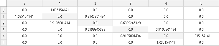
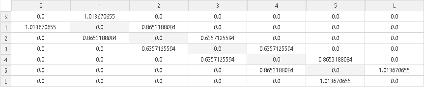
Using these specifications in FD3D, we obtain a coupling matrix for this response as shown in Fig. 1. We shall use this coupling matrix as target during the complete design procedure.
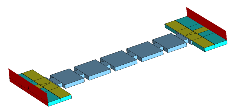
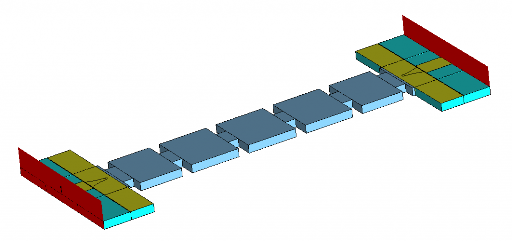
We have selected the following basic elements to build the SIW filter shown in Fig 2:
- Resonators: rectangular resonators in which the electric walls are implemented by means of via-holes.
- Internal couplings: rectangular irises in which the electric walls are implemented with via- holes.
- External couplings: tapered microstrip-to-SIW transition.
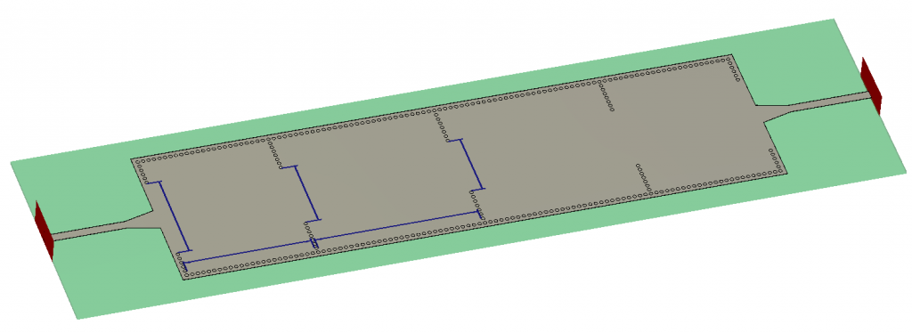
We have obtained the initial dimensions of each component through quick Eigenmode simulations. Then, we have assigned a design parameter per component (indicated by the dimension lines (blue) in Fig. 2) to control the individual mechanisms associated with the coupling matrix:
- The length of the rectangular resonators
- The width of the inter-cavity irises
- The width of the input/output iris at the microstrip-to-SIW transitions.
In Fig. 3, we show the variation of each coupling matrix element within the range defined for the physical design parameter.
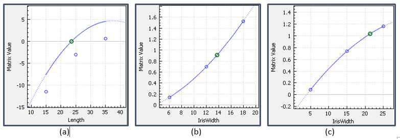
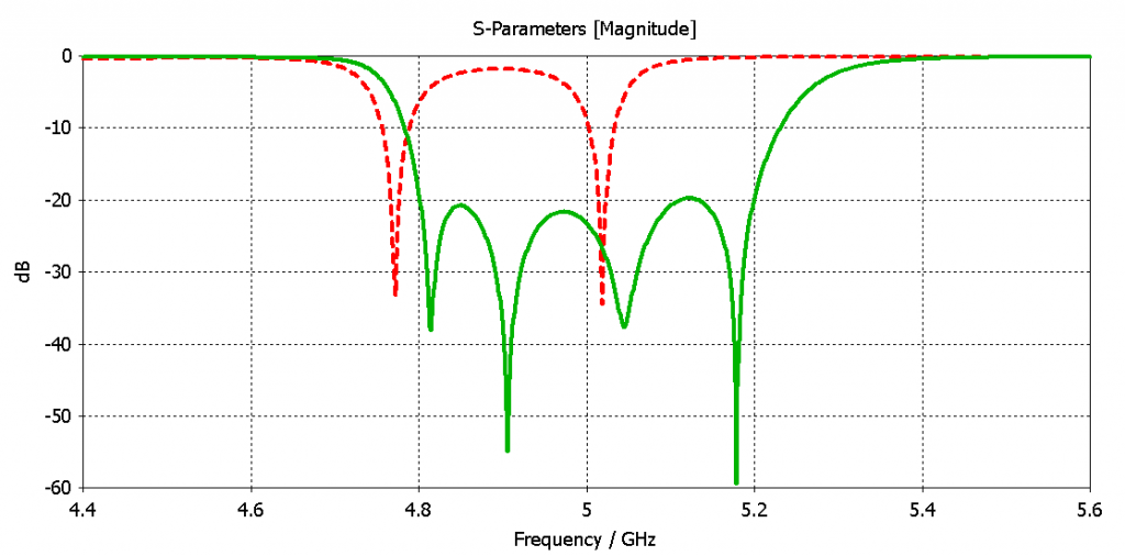
For the initial design, FD3D selects the appropriate dimensions according to these curves for the individual coupling matrix entries. The initial response (indicated by the red dashed curve in Fig. 4) deviates from the target due to loading effects not considered in the eigenmode analysis. To solve this, we launch the space mapping ad-hoc optimization included in FD3D. This algorithm extracts the coupling matrix from the S-parameters and calculates a new set of parameter values based on the curves in Fig. 3. The result of this ad-hoc procedure is shown by the green solid curve in Fig. 4, where the desired filter response of the synthesis is achieved.
ESIW filter design workflow
In the case of ESIW filters, we can take advantage of specific solvers for waveguide technology, which speed up the analysis significantly. Then, the workflow we introduce for the ESIW involves two additional ingredients: Fest3D and CST Studio Suite® optimization based on the coupling matrix extraction from FD3D. The objective is to design the filter shown in Fig. 5. The filter consists of the external port couplings (microstrip-to-ESIW transition) and cavity resonators that are realized in rectangular waveguide technology. The workflow is outlined in the following steps:
- Define the filter specifications in FD3D and select from a range of topologies that would provide the appropriate coupling matrix for the synthesis and final optimization.
- Generate a rectangular waveguide bandpass filter using the automated synthesis wizard in Fest3D.
- Design the microstrip-to-ESIW transition with CST Studio Suite® by using the Eigenmode solver.
- Connect the two parts (transition + waveguide filter) in CST Studio Suite® Circuits & Systems and execute the optimizer based on the extraction of the coupling matrix, where the FD3D project in step 1 is selected as the goal.
The filter specifications that we have selected in this case are:
- Centre frequency: 20 GHz
- Bandwidth: 500 MHz
- Return loss: 25 dB
- Number of poles: 5
Using these specifications in FD3D, we obtain the corresponding coupling matrix as shown in Fig. 6.
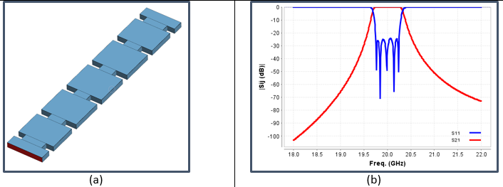
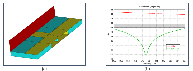
We have designed the waveguide filter using the Fest3D automatic design tool for inductive bandpass filters. We have selected as port the standard rectangular waveguide WR-42. However, the key of the ESIW filter design is to simplify the connection of the filter to the transition by using the same filter height as the thickness of the substrate of the transition (see Fig. 5). In this case, we have chosen a substrate with a thickness of 1.524 mm [2], which is then the height of the filter as shown in Fig. 7 (a). Using the automatic design tool, we have obtained the response in Fig. 7(b), which perfectly meets the specifications. Note that this is obtained without the need for additional optimization.
After that, we have designed the microstrip-to-waveguide transition as shown in Fig. 8 (a) [2]. We have obtained an initial response (red curve in Fig. (b)) that we have optimized to provide an input match better than 35 dB in the frequency band of interest (green curve in Fig. (b)).
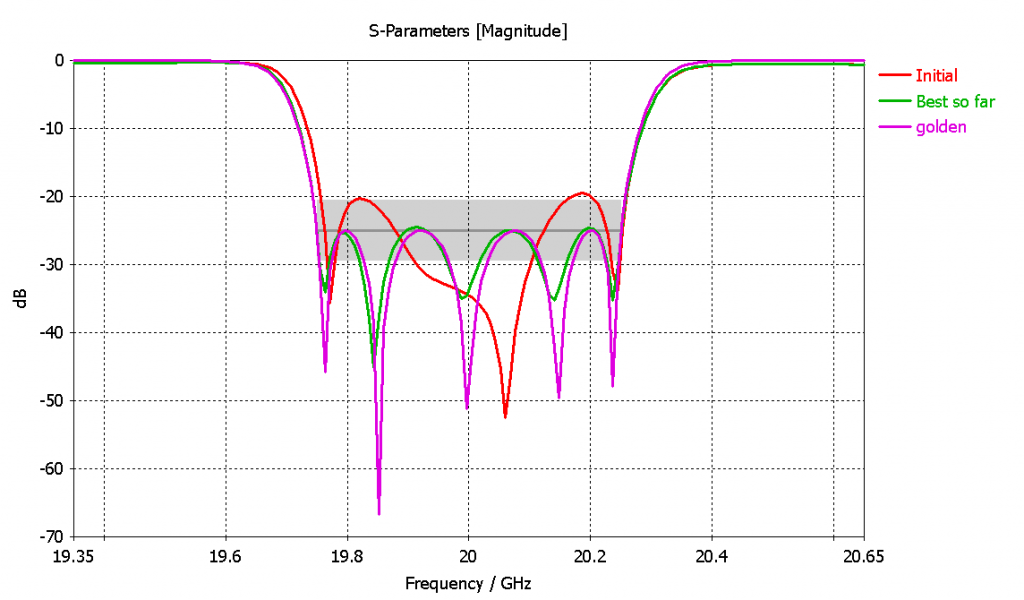
The next step is to connect the waveguide filter to the input/output transition. To do so, we have used CST Studio Suite® Circuits & Systems, which is able to connect electromagnetically both parts by means of the EM modes at the interfaces. We then obtain the result shown by the red curve in Fig. 9. The result is already quite close to the golden (ideal) response because we have designed the transition to have a very good matching and, as already said, the interface of the transition and the filter have the same dimensions (no mismatch is added). Finally, we optimize the component using CST Studio Suite® optimizer coupled to FD3D, i.e., instead of using the S-parameters as goal function for the optimizer, we use the ideal coupling matrix (See Fig. 6). In addition, to do this final optimization we only need to tune the waveguide filter, not the transition. Therefore, the optimization process is very efficient because we compute the waveguide filter with the Fest3D EM modal solver, and the transition block is not recomputed from iteration to iteration. The final response has an ideal equal ripple as seen from the green curve in Fig. 9.
Summary
In this blog post, we have shown how to combine different tools and techniques within CST Studio Suite® environment to design microwave filters. We have successfully applied these workflows to the design of two particular filters based on SIW and ESIW technologies.
References
[1] D. Deslandes and K. Wu, “Integrated microstrip and rectangular waveguide in planar form,” IEEE Microwave Wireless Component Letter, vol. 11, no. 2, pp. 68–70, Feb. 2001.
[2] A. Belenguer, H. Esteban, and V. E. Boria, “Novel Empty Substrate Integrated Waveguide for High-Performance Microwave Integrated Circuits”, IEEE Transactions on Microwave Theory and Techniques, Vol. 62, No. 4, April 2014.
Discover extensive Electromagnetics resources and connect with other Electromagnetics experts in our SIMULIA Community.

SIMULIA offers an advanced simulation product portfolio, including Abaqus, Isight, fe-safe, Tosca, Simpoe-Mold, SIMPACK, CST Studio Suite, XFlow, PowerFLOW and more. The SIMULIA Community is the place to find the latest resources for SIMULIA software and to collaborate with other users. The key that unlocks the door of innovative thinking and knowledge building, the SIMULIA Community provides you with the tools you need to expand your knowledge, whenever and wherever.

Dr. Carlos Vicente currently serves as Senior Technical Sales Manager for Aurorasat, part of SIMULIA, a Dassault Systémes brand. Dr. Vicente received his Ph.D. in telecommunications engineering in 2005 from the Technical University of Darmstadt, Germany. In his doctoral thesis, Dr. Vicente researched high power effects in communications satellites such as RF breakdown and passive intermodulation. In 2006, he co-founded the company Aurora Software and Testing S. L. (Aurorasat).