
“Why don’t my simulation results agree with the measurement?” This is the question I sometimes heard from our customers and which inspired us to start CST Lab, which is a project that promotes the combination of simulation and measurement to fix the perennial problem of mismatched results. CST Lab was officially started two years ago, and for the past 5 years we have been working in this space with our joint workshops with Rohde & Schwarz, one of the global leaders in measurement instruments and techniques. These workshops were very well received since the content went well beyond a typical product presentation. The workshops examine critical points in the design process and include hands-on learning for both measurement and simulation portions.
Recently, we introduced a two-day vector network analyzer (VNA) training course, which covers the fundamentals of microwave measurement and the obtained measured data are used during the second day for the material characterization and component modeling.
Providing customers with comprehensive technical support
CST Lab’s objective is to provide our customers with broader, application-based technical support where we deal with the overall design process instead of limiting the support to the simulation portion only.
CST Lab supports our customers who can benefit from our extensive knowledge concerning measurement and its interpretation. The approach is beneficial to all engineers who need to reduce the length of the design cycle making the design process more robust and reliable.
Benefits of combining simulation and measurement
There are many benefits of combining simulation and measurement during the design stage. Each of the domains is suitable for different tasks. For instance, simulation allows us to do what-if analysis without the expensive and lengthy manufacturing process. We can employ an automatic optimization engine to improve the device parameters. Also, simulation provides an inside view of EM field visualization, which provides a better understanding of the physical mechanisms.
On the other hand, material properties, which are the critical input information for 3D EM simulation, need to be determined using the measurement of a simple, well-defined sample. Measurement is usually very fast, providing the results in real-time. Also, the measurement contains all the physical effects of the device under test (DUT). So if we combine both domains, we can always be sure we have used the best-suited tool for the particular task.
Common misconceptions
There are a few common misconceptions or mistakes that we encounter and correct when we are working with users or giving workshops on simulation and measurement. The most common mistake is that people simulate something different than what is measured. A typical case is a microwave circuit or antenna that includes an adapter is measured, but because the engineer assumes the adapter behaves ideally, it is not included in the 3D model. However, if we look closer and measure its S-parameters, the results show that the troublemaker is in fact, the adapter. The adapter in this example can be replaced with any other piece of structure that is present in the experiment, but it is missing in the virtual model. Sometimes, a very tiny detail might cause a significant discrepancy, and it can be challenging to reveal this.
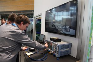
If we look at electromagnetic compatibility (EMC), we can find an example of a typical misconception. A standard initial request of a potential customer dealing with an EMC issue is: “Please put all the system including all the nonlinear circuits and mechanical parts into the 3D EM simulator and show us the agreement of emissions to our measurement”. This is a very inefficient approach since it would require a lot of time to transfer all the complexity of the device to the virtual model including, possibly, the effects of the environment where the device being tested was measured. Regardless, this approach won’t help to solve the EMC issue if the aim is just to replicate the measurement with the simulation. Instead, we recommend capturing only the most relevant portion for the principal study and finding the emission sources utilizing field visualization. As soon as we understand the how the emissions are generated, we can take action to suppress them. Typically that can be achieved just by modifying the PCB layout. Then, we may add a bit more complexity in the final step before applying changes to the physical sample to complete the verification loop.
The future of CST Lab
Our efforts with CST Lab are well received, and our customers actively cooperate since they see the benefits of combining measurement and simulation.
During the last three years, we have developed several novel workflows that speed up the design process and which enable our customers to create much more robust virtual models with an accuracy we haven’t seen before. Besides the development of further new approaches, the most critical task and challenge for the future will be the transfer of this knowledge to technical practice. In fact, CST recently jointly presented a course from the well-respected European School of Antennas titled “Combination of Measurement and Simulation.” This is a wonderful example of companies and academia coming together to promote this approach to design.
Want to learn more? Check out these webinars in our archive and sign up with MyCST to be notified of upcoming training, workshops and other CST Lab related events
Related webinars:
Precise Characterization of Multipin Connectors

Vratislav Sokol received his M.Sc. and Ph.D. degrees in radioelectronics from the Czech Technical University in Prague in 2000 and 2004, respectively. He was a post-doctoral research associate with Cork Institute of Technology in Ireland where he dealt with an ultra-wideband transceiver. His activities are focused on microwave circuit design and modeling using electromagnetic field simulators and precise microwave measurement and calibration. He has been with CST since 2006 as a Senior Application Engineer.